- Authors: P. Azunre, C. Rotschild, M. Baldo, G. Verghese, S. G. Johnson
- Sponsorship: Center for Excitonics
Given recent advances in the field of global optimization, we aim to make advances towards deterministic global optimization of some important engineering systems (namely, multilayer filters, lens systems, and semiconductors),. The design of these systems is an activity popularly regarded as an art, and it may potentially be turned into a science using the deterministic global optimization technique of branch-and-bound. The technique of branch-bound is briefly illustrated in Figure 1 below.

Figure 1: An illustration of the technique of branch-and-bound.
As Figure 1 shows, this methodology requires the cheap construction of tight bounds on the merit function defining each optimization problem. With the recent availability of extensively verified and parallelizable software for suppressing the dependency problem (using the technique of Taylor arithmetic) arising in attempts to bound explicit merit functions (of sufficient differentiability), we aim to identify the subset of the important classes of multilayer filters and lens systems accessible by rigorous global optimization. Given recent advances in mathematical theory for constructing parametric bounds on ODE solutions (in particular, suppressing the wrapping effect using the technique of generalized McCormick Relaxations), we have developed a mathematical methodology for constructing parametric bounds on semilinear parabolic PDE solutions. The specific long-term goal of the PDE work is rigorous global optimization of semiconductors. The project is presently in the supercomputing software development phase. Preliminary serial work in the domain of multilayer filters yielded an important broadband omnidirectional antireflection coating design for silicon solar cells. Work is in progress to experimentally demonstrate this design.
- Authors: M. E. Bahlke, H. A. Mendoza, M. A. Baldo
- Sponsorship: MITEI Graduate Fellowship in Energy, Center for Excitonics, DOE Office of Basic Energy Sciences EFRC
Photolithography’s accuracy and scalability have made it the method for sub-micron-scale definition of single-crystal semiconductor devices for over half a century. Unfortunately, organic semiconductor devices are chemically incompatible with the types of resists, solvents, and etchants traditionally used. This work investigates the use of an uncommonly used chemically inert resist method [] [] [] [] [] that relies on physical phase changes for lift-off patterning of thin films of organic semiconductors and metals.
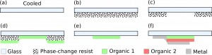
The resist gas is flowed over a cryogenically cooled substrate, where it freezes solid as schematically shown in Figure 1. This layer an be patterned by thermal excitation in a number of ways to define the areas where the desired thin film is to remain. After the desired thin film or films are deposited, the substrate is brought up above the resist material’s sublimation point, leaving behind only the intended pattern. All the unwanted regions are lifted-off by the subliming resist.
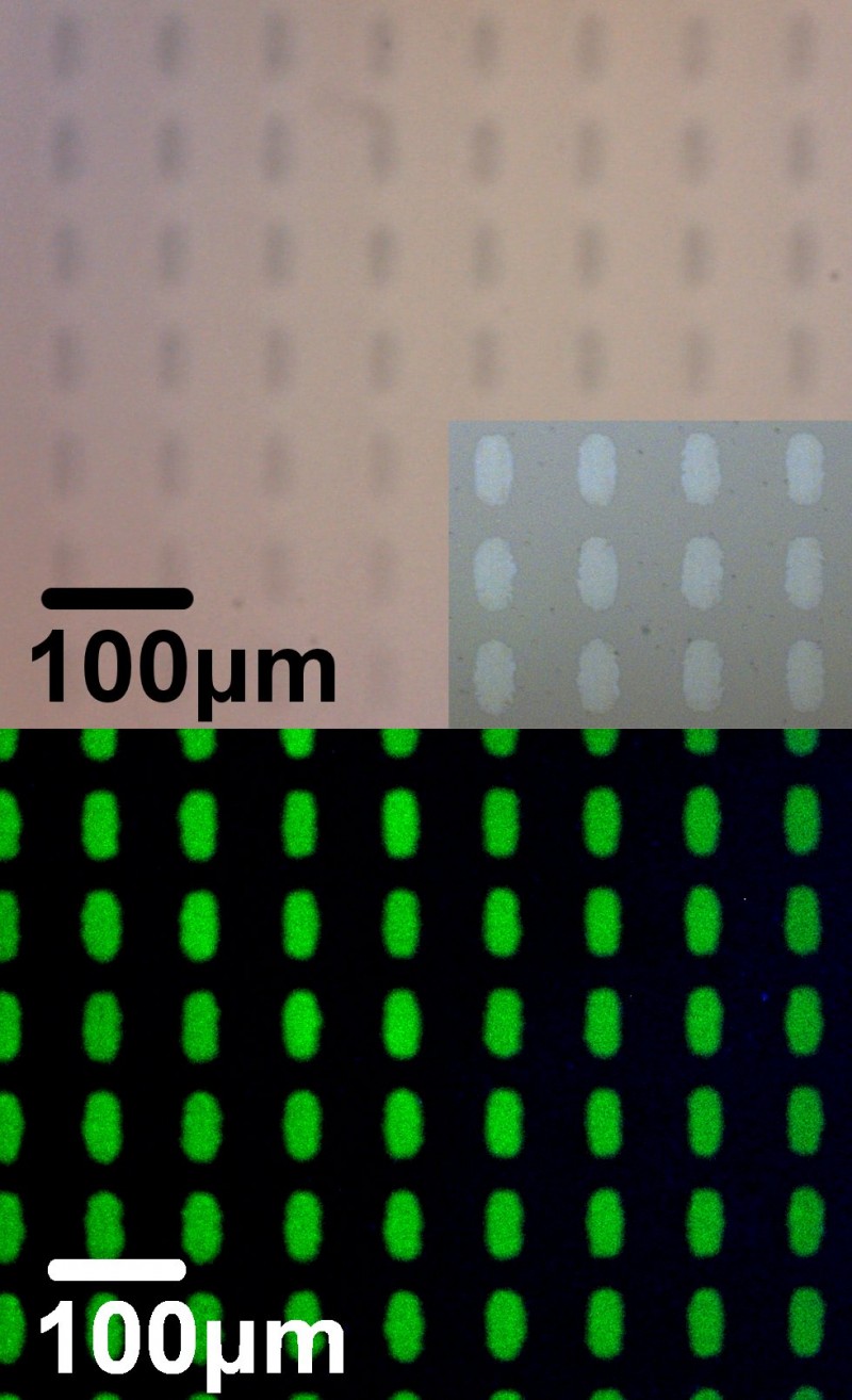
Creating and defining the shadow mask on the surface of the substrate in this manner allow for patterning it with a stamp or roller with micron-scale features without changing the process conditions. In this work, carbon dioxide is used as the sublimable mask material, and prototype stamps have been fabricated using SU-8 photoresist. A mask and the subsequent organic thin film are shown in Figure 2. This process may provide an alternative to shadow masks and provide a manufacturing solution for large area organic electronics.
-
-
Figure 1: Simplified process flow for sublimation lithography (not to scale). (a) Begin with a cooled substrate to facilitate resist deposition. (b) Deposit resist. (c) Selectively pattern resist. (d) Deposit desired thin film. (e) Lift-off resist leaving patterned thin film. (f) Repeat as necessary to complete device.
-
-
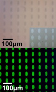
Figure 2: Optical micrograph (top) of a patterned sublimable mask of carbon dioxide. The inset in the lower right-hand corner shows the resulting organic thin film after deposition and lift-off. The photoluminescence (bottom) of the same patterned film.
- Authors: V. R. Manfrinato, L. Zhang, D. Su, H. Duan, E. A. Stach, K. K. Berggren
- Sponsorship: Center for Excitonics, Energy Frontier Research Center funded by the U.S. Department of Energy, Office of Science (DE-SC0001088); Brookhaven National Laboratory
Electron-beam lithography (EBL) readily enables the fabrication of sub-10-nm features [] . However, the resolution limits of this technique at length scales for below 10 nm are not well understood. The known resolution limiting factors of EBL are: (1) electron scattering; (2) spot size; (3) development process; and (4) resist structure. We decided to minimize the influence of electron scattering by using 200-keV electrons. We used Si3N4membranes as the substrate to minimize backscattered electrons. To minimize the spot size, we chose an aberration-corrected scanning transmission electron microscope (STEM) as the exposure tool with 0.14-nm spot size. STEM exposures at 200 keV have been done in conventional resists before [] [] , resulting in feature sizes of 6 nm and resolution (i.e., pattern period) of 30 nm. However, the resolution-limiting factors were not systematically explored. In this work we did STEM exposures in 10-nm-thick hydrogen silsesquioxane (HSQ) at 200 keV. We developed the structures with salty development [] and performed bright field TEM metrology [] .
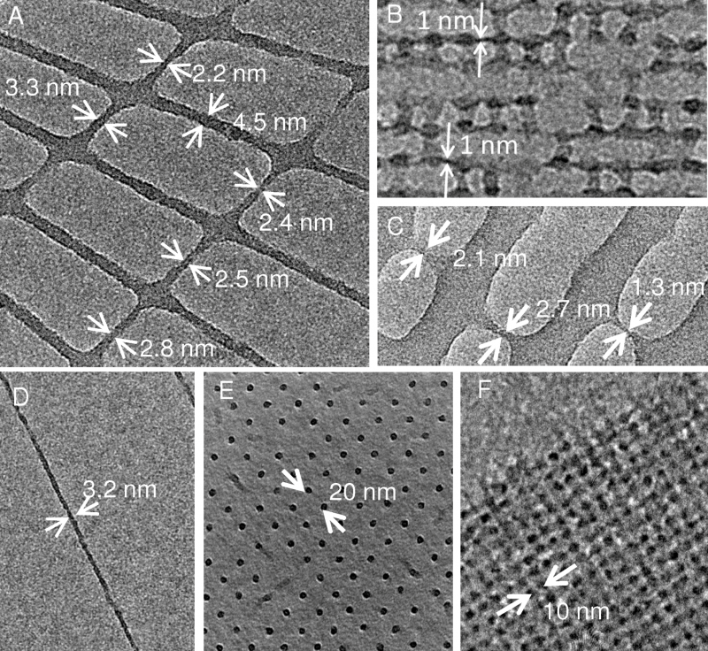
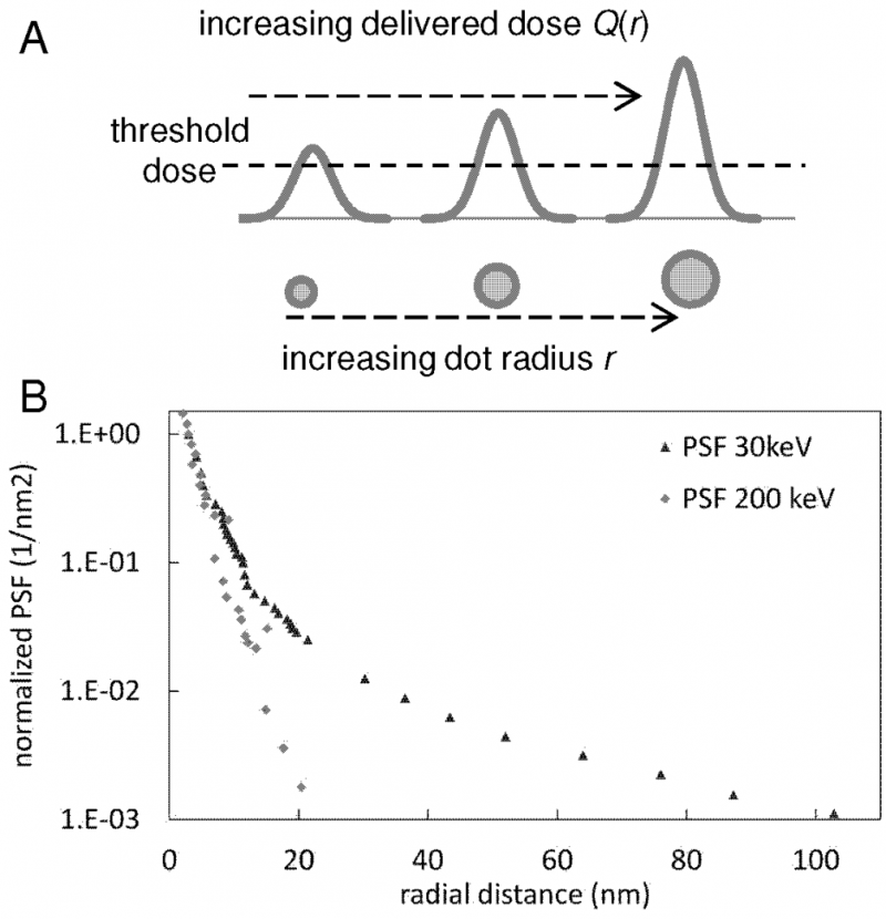
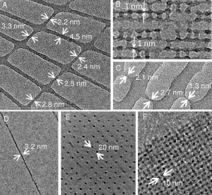
Figure 1 shows feature sizes from 1 to 3 nm and maximum resolution of 10-nm pitch, which represent the smallest structures written in conventional e-beam resists. The reduced spot size in the STEM was responsible for the minimum feature size achieved. In addition, we measured the point-spread function (PSF) at 200 keV, shown in Figure 2. The PSF at 200 keV is much narrower than the 30keV one in the small radius range, leading to smaller short-range proximity effect and thus higher resolution.
-
-
Figure 1: Bright field transmission electron micrographs HSQ structures exposed at 200 keV. The HSQ thickness was 10-15 nm and it was on top of a 10-nm-thick Si3N4 membrane. The linear-dose was 30 nC/cm (20,000 electrons/nm). The exposure step size was 1-2 nm. (A), (B), and (C) show the minimum feature sizes obtained by this method. (D) shows an isolated 3-nm-wide structure over a micron long. (E) and (F) show 10- and 5-nm-half-pitch dot array of HSQ. The doses were 15 and 9 fC/dot, respectively.
-

-
Figure 2: The point-spread function (PSF) for 10-nm-thick HSQ at 30 keV and 200 keV on top of Si3N4 menbrane. (A) shows the method to measure the PSF by using single pixel exposures. Given a constant threshold of dose density, as the pixel dose increases the radius increases. This series of dots probe the energy density distribution into the resist at different radii, leading to the PSF. (B) Experimental PSFs at 30 and 200 keV. It is clear that the 200keV PSF has a narrower spread than the 30keV one.