Recombination Dynamics of Charge Carriers in Nanostructured Solar Cells
Nanostructured solar cells are attracting increasing attention as a promising photovoltaic (PV) technology [1] . Generation of free charge carriers in nanostructured PV devices occurs at the electron donor-acceptor interface, analogous to the pn-junction interface in traditional crystalline silicon solar cells. However, recombination at this interface constitutes one of the major charge carrier loss pathways. Thus characterizing and controlling recombination dynamics is critical for informing the design of novel device architectures. Recombination parameters also enable comparisons between different device architectures.
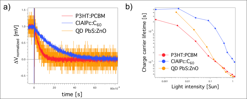
In this work, we employ the transient photovoltage (TPV) technique [2] to probe recombination mechanisms under standard operating conditions in three different solar cells, as shown in Figure 1: a poly(3-hexylthiophene) and phenyl-C61-butyric acid methyl ester (P3HT:PCBM) bulk heterojunction; a chloroaluminium phthalocyanine and fullerene (ClAlPc:C60) planar mixed heterojunction; and a lead sulfide quantum dot and zinc oxide (QD PbS:ZnO) pn-heterojunction. The normalized TPV data acquired at 0.5-sun illumination intensity are shown in Figure 2a, which compares the recombination lifetimes of charge carriers in these devices. The observed differences in carrier lifetimes may arise from variations in the respective interface morphologies: for example, the slower recombination transients observed in the ClAlPc:C60 device may be attributed to the intrinsic planarity of this particular architecture. We can also measure the charge carrier lifetime as a function of the light intensity, as shown in Figure 2b; this result confirms that recombination dynamics are faster in P3HT:PCBM and QD PbS:ZnO than in ClAlPc:C60 PV devices.
-
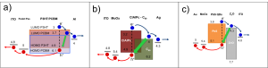
- Figure 1: Energy level (in eV) of the PV architectures studied. The blue (red) dots and arrows represent the (holes) electrons and their pathway to the (anode) cathode. Green arrows represent the recombination pathways. a) P3HT:PCBM – between a layer of poly(3,4-ethylenedioxythiophene) poly(styrenesulfonate)–Pedot:pss–and ITO and Al as electrodes. b) ClAlPc:C60–between a layer of molybdenum oxide–MoOx–and ITO and Ag as electrodes. c) PbS QD:ZnO–between a layer of MoOx –and Au as anode and ITO as electrodes.
-
- Figure 2: a) Normalized transient photovoltage data acquired at 0.5 Sun for P3HT:PCBM, ClAlPC:C60 and PbS QD:ZnO solar cells. b) Charge carrier lifetime as a function of the light intensity for P3HT:PCBM, ClAlPC:C60, and PbS QD:ZnO solar cells.
- Anonymous, “A sunny outlook,” Nature Photonics, vol. 6, no. 3, p. 129, Mar. 2012. [↩]
- C. G. Shuttle, B. O’Regan, A. M. Ballantyne, J. Nelson, D. D. C. Bradley, J. de Mello, and J. R. Durrant, “Experimental determination of the rate law for charge carrier decay in a polythiophene: Fullerene solar cell,” Applied Physics Letters, vol. 92, p. 3, 2008. [↩]
