Scalable 3-D Microelectrode Recording Architectures for Characterization of Optogenetically Modulated Neural Dynamics
- Category: Optics & Photonics
- Tags: clifton fonstad, ed boyden, joerg scholvin
Optogenetics is commonly used for precision modulation of the activity of specific neurons within neural circuits [1] , but assessing the impact of optogenetic neuromodulation on the neural activity of local and global circuits remains difficult. Our collaborative team recently initiated a project (Scholvin et al., SFN 2011) to design and implement 3-D silicon-micromachined electrode arrays with customizable electrode locations, targetable to defined neural substrates distributed in a 3-D pattern throughout a neural network in the mammalian brain and compatible with simultaneous use of a diversity of existing light-delivery devices.
We have developed a series of innovations aimed at facilitating the scalability aspect of these probes, i.e., aspects of probe design that should enable them to scale to 1000 channels of neural recording or more. First, we have developed streamlined electrode fabrication methodologies that enable micromachined probes to be first fabricated using conventional silicon micromachining, then rapidly assembled into custom 3-D arrays, with semi-automated formation of the necessary electrical connections and mechanical constraints. Second, we have developed a set of surgical and insertion technologies towards the goal of enabling the insertion of electrode arrays with a high number of electrode shanks into the brain, while minimizing probe insertion damage. Finally, to facilitate scaling of the channel count beyond what is feasible with external amplifiers, we are exploring new approaches for integration of amplifier circuits directly on the probe arrays themselves, to remove bottlenecks associated with connecting of probes to the outside world.
-

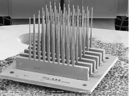
- Figure 1: A scanning electron micrograph of six 10-probe linear arrays assembled into a 6 x 10 two-dimensional array of probes. The probes in this figure and in Figure 2 were fabricated for assembly studies and have no sense electrodes. Each needle is 3.5 mm long and 40 µm wide at the tip.
-
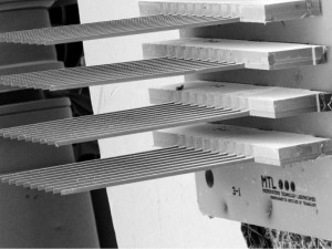
- Figure 2: A close-up scanning electron micrograph of a portion of the array in Figure 1. The needles are thinned to 40 µm and are spaced 400 µm center-to-center in each linear array. The linear arrays are spaced at 600 µm. The above structure was fabricated using 300-µm thin wafers.

- X. Han and E. S. Boyden, “Multiple-color optical activation, silencing, and desynchronization of neural activity, with single-spike temporal resolution,” PLoS ONE, vol. 2, no. 3, p. e299, Mar. 2007. [↩]