Investigating the Resolution Limits of 200-keV Electron-beam Lithography with an Aberration-corrected STEM
- Category: Nanotechnology
- Tags: center for excitonics, karl berggren, vitor manfrinato
Electron-beam lithography (EBL) readily enables the fabrication of sub-10-nm features [1] . However, the resolution limits of this technique at length scales for below 10 nm are not well understood. The known resolution limiting factors of EBL are: (1) electron scattering; (2) spot size; (3) development process; and (4) resist structure. We decided to minimize the influence of electron scattering by using 200-keV electrons. We used Si3N4membranes as the substrate to minimize backscattered electrons. To minimize the spot size, we chose an aberration-corrected scanning transmission electron microscope (STEM) as the exposure tool with 0.14-nm spot size. STEM exposures at 200 keV have been done in conventional resists before [2] [3] , resulting in feature sizes of 6 nm and resolution (i.e., pattern period) of 30 nm. However, the resolution-limiting factors were not systematically explored. In this work we did STEM exposures in 10-nm-thick hydrogen silsesquioxane (HSQ) at 200 keV. We developed the structures with salty development [1] and performed bright field TEM metrology [4] .
Figure 1 shows feature sizes from 1 to 3 nm and maximum resolution of 10-nm pitch, which represent the smallest structures written in conventional e-beam resists. The reduced spot size in the STEM was responsible for the minimum feature size achieved. In addition, we measured the point-spread function (PSF) at 200 keV, shown in Figure 2. The PSF at 200 keV is much narrower than the 30keV one in the small radius range, leading to smaller short-range proximity effect and thus higher resolution.
-
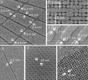
- Figure 1: Bright field transmission electron micrographs HSQ structures exposed at 200 keV. The HSQ thickness was 10-15 nm and it was on top of a 10-nm-thick Si3N4 membrane. The linear-dose was 30 nC/cm (20,000 electrons/nm). The exposure step size was 1-2 nm. (A), (B), and (C) show the minimum feature sizes obtained by this method. (D) shows an isolated 3-nm-wide structure over a micron long. (E) and (F) show 10- and 5-nm-half-pitch dot array of HSQ. The doses were 15 and 9 fC/dot, respectively.
-

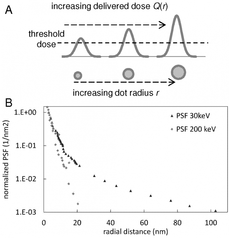
- Figure 2: The point-spread function (PSF) for 10-nm-thick HSQ at 30 keV and 200 keV on top of Si3N4 menbrane. (A) shows the method to measure the PSF by using single pixel exposures. Given a constant threshold of dose density, as the pixel dose increases the radius increases. This series of dots probe the energy density distribution into the resist at different radii, leading to the PSF. (B) Experimental PSFs at 30 and 200 keV. It is clear that the 200keV PSF has a narrower spread than the 30keV one.
- J. K. W. Yang and K. K. Berggren, “Using high-contrast salty development of hydrogen silsesquioxane for sub-10-nm half-pitch lithography,” Journal of Vacuum Science & Technology B, vol. 25, no. 6, pp. 2025-2029, Dec. 2007. [↩] [↩]
- C. Vieu, F. Carcenac, A. Pépin, Y. Chen, M. Mejias, A. Lebib, L. Manin-Ferlazzo, L. Couraud, and H. Launois, “Electron beam lithography: Resolution limits and applications,” Applied Surface Science, vol. 164, pp. 111-117, Aug. 2000. [↩]
- S. Yasin, D. G. Hasko, and F. Carecenac, “Nanolithography using ultrasonically assisted development of calixarene negative electron beam resist,” Journal of Vacuum Science & Technology B, vol. 19, no. 1, pp. 311-313, Jan. 2001. [↩]
- H. Duan, V. R. Manfrinato, J. K. W. Yang, D. Winston, B. M. Cord, and K. K. Berggren, “Metrology for electron-beam lithography and resist contrast at the sub-10-nm scale,” Journal of Vacuum Science & Technology B, vol. 28, no. 6, pp. C6H11-C6H17, Dec. 2010. [↩]