Graphene Nanoribbons for Flexible Digital Circuits
- Category: Circuits & Systems
- Tags: yi song
Today, power dissipation is one of the most important limiting factors in digital circuit design. As devices scale further and processing becomes more challenging, novel materials may be necessary to further advance the low-power paradigm. Graphene is a fascinating nanostructure that has attracted much attention over the past several years due to its extraordinary mechanical and electrical properties. Graphene-based mixers and other RF circuits have been investigated, but graphene transistors (GFETs) are current not viable for digital applications. One of the main limitations of GFETs is its extremely poor on/off current ratio (typically less than 2).
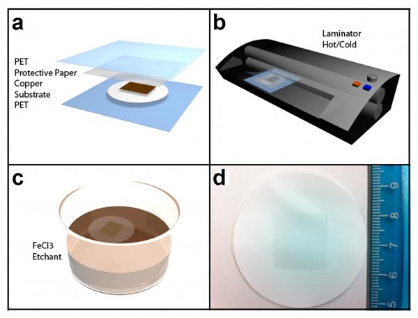
It is well known that the on/off ratio improves drastically as dimensions reach ~15nm, which is believed to be due to quantum confinement; values as high as 106 have been reported [1] . Patterning graphene nanoribbons on flexible substrates may make it possible to realize flexible digital electronics. We have developed a technique to quickly and reliably transfer Chemical Vapor Deposition (CVD) graphene onto a variety of flexible substrates such as Teflon, vinyl, and cellulose acetate/cellulose nitrate, as illustrated in Figure 1. It is currently unknown whether the same electrical behavior will be observed on a flexible substrate. Other challenges include developing techniques to smooth the edges of lithographically defined nanoribbons and controllably shifting the low-conduction point.

Figure 1: Steps for direct transfer lamination technique. (a) The graphene/copper is placed on the substrate and pressed between two PET films. (b) The stack is inserted into a lamination machine. (c) Substrate/graphene/copper is placed in a copper etch solution. (d) Graphene on a PTFE filter.
- X. Wang, Y. Ouyang, X. Li, H. Wang, J. Guo, and H. Dai, “title,“ Phys. Rev. Lett. 100, 206803 (2008). [↩]