Development of Nanostructured Optical Field Emitter Arrays
- Category: Optics & Photonics
- Tags: karl berggren, luis velasquez-garcia, yujia yang
We are interested in the application of arrays of electron field emitters, which can be achieved from a variety of materials, for the preparation of compact and coherent X-ray sources via inverse Compton scattering. Field emission of electrons is commonly achieved by applying a static electric field or optical illumination to sharp metal tips. Sub-wavelength nanostructures can provide geometry-dependent electric field enhancement for both methods. For applications in coherent X-ray sources, the field emitter arrays should be able to emit short electron pulses, typically on the femtosecond timescale, which is difficult using conventional electrical circuits. Therefore, optical triggering, whereby a femtosecond laser is used to stimulate electron emission, has been considered.
We have simulated optical fields around various field emitter structures using COMSOL finite element software. Among them, we are particularly interested in the “bullet” structure illustrated in Figure 1. Conical tip structures are widely used to achieve both electrostatic and optical field enhancement in field emitters; however, uniform conical structures pose significant challenges in nanoscale fabrication due to their tapered geometry. Arrays of metallic “bullet” structures, as shown in Figure 1, may be fabricated with a high areal density via positive-tone electron beam lithography with a PMMA resist.
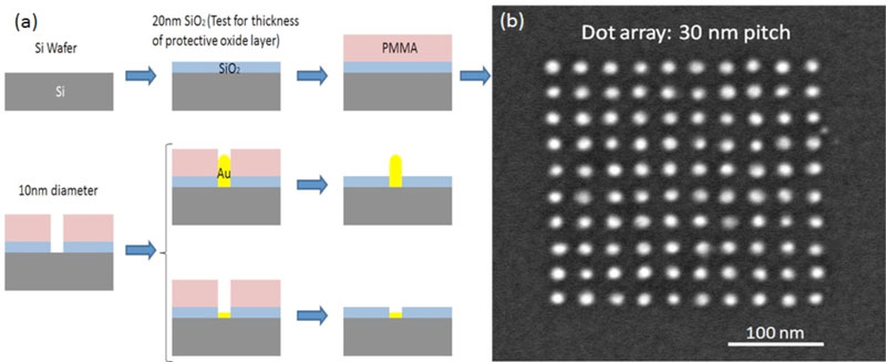
We have designed a fabrication process for the preparation of arrays of optical-field emitters, based on the metallic “bullet” structure shown in Figure 2 (a). The thin SiO2 layer shown in Figure 2 (a) is used to prevent electron emission from the bulk silicon substrate by acting as an electrically insulating barrier. The thickness of the SiO2 layer has yet to be optimized. As a proof of concept, we have fabricated an array of Au nanoparticle emitters with an aspect-ratio of 1 (see Figure 2 (b)). Further optimization of the fabrication process is currently underway.
-
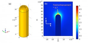
- Figure 1: Gold bullet optical-field emitter. (a) Emitter geometry; (b) 2-D electric field amplitude map in a plane of the emitter axis. Radius of the cylinder and hemispherical tip is 5 nm. Cylinder length is 30 nm. The illumination source has a wavelength of 810 nm. Gold ( =-24.9+1.57i) and water ( =1.77) are chosen as tip and dielectric materials, respectively. The optical triggering field propagates in x-direction (from left to right) and is polarized along the y-axis (in-plane and along the tip axis). Propagation (k) and polarization (E) directions are shown as arrows. The field enhancement displayed in (b) is normalized with respect to the incident optical field and has a peak enhancement factor ~3.7 at the apex of the “bullet”.

-
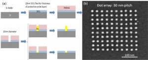
- Figure 2: (a) Fabrication process of the gold optical-field emitters. The process starts from a Si wafer. A thin SiO2 layer is grown, preventing electron emission from bulk Si. Electron beam lithography and etching produces a patterned oxide layer. Au deposition and PMMA lift-off allows creation of Au “bullet” arrays. The aspect-ratio of the emitters depends on the Au deposition time. The Si substrate can be electrically grounded to serve as an electron reservoir, or connected to a DC bias to perform electron emission induced by a combination of electrostatic field and optical field stimulation. (b) SEM image of a Au dot array. An oxide layer was not deposited on this sample and the gold dots (aspect-ratio of 1) are deposited directly on the Si wafer. The diameter of each gold dot is 10 nm and the dot pitch is 30 nm. A total of 100 Au dots are packed within an area of less than 0.1 μm2.
- D. Temple, “Recent progress in field emitter array development for high performance applications,” Materials Science and Engineering: R: Reports, vol. 24, pp. 185-293, Jan. 1999.
- O. J. F. Martin and C. Girard, “Controlling and tuning strong optical field gradients at a local probe microscope tip apex,” Applied Physics Letters, vol. 70, pp. 705-707, Feb. 1997.
- L. Novotny, R. X. Bian, and X. S. Xie, “Theory of nanometric optical tweezers,” Physical Review Letters, vol. 79, pp. 645-648, July 1997.