A Two-step Pipelined Triple-slope ADC
- Category: Circuits & Systems
- Tags: hae-seung lee, miguel perez
High resolution and high speed in data converters are difficult to achieve at low power consumption levels [1] . This is due to the fundamental limit imposed by thermal noise in high-resolution converters, among other factors. In order to increase the resolution of a thermal noise limited data converter by one bit while maintaining the same sampling frequency, the power consumption must quadruple [2] . Therefore, it is advantageous to exploit the benefits provided by multiple converter architectures in order to create the most energy-efficient design possible.

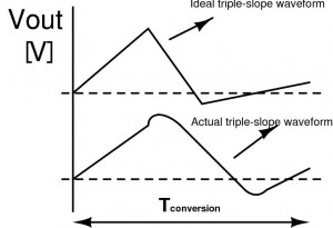
Figure 1: Output waveforms for the integrator used in the triple-slope architecture. Top waveform depicts ideal operation while the bottom waveform shows nonlinearity due to the OTA’s finite transconductance.
In this project, we explore the advantages provided by combining aspects from three standard data converter architectures. The current design aims to achieve at least 16-bit linearity and at most an FOM of 100 [fJ/conv-step] by implementing a two-step pipeline triple-slope ADC. This implementation takes advantage of the high linearity provided by integrating converters combined with the speed improvements inherent in the triple-slope, two-step and pipeline architectures [3] .
An important limitation in a standard triple-slope architecture that leads to non-linearity when operated at high speeds is the finite gain or transconductance of the Opamp or operational transconductance amplifier (OTA), respectively, employed in the integrator. This particular non-ideality, as depicted in Figure 1, causes an input-dependent transient in the output waveform of the triple-slope integrator at every switching point, which results in a decrease in the converter’s overall linearity. To mitigate this problem, we are investigating a current cancellation technique that relieves the amplifier from having to supply the current to the integrating capacitor. This technique effectively increases the OTA’s transconductance as seen from the input node, ultimately producing an output waveform closer to the ideal version in Figure 1.
- B. Murmann, “ADC Performance Survey 1997-2012,” [Online]. Available: http://www.stanford.edu/~murmann/adcsurvey.html. [↩]
- H. S. Lee, and C. G. Sodini, “Analog-to-Digital Converters: Digitizing the Analog World” Proc. IEEE, vol. 96, no. 2, pp. 323-334, Feb. 2008. [↩]
- F. Maloberti, Data Converters. The Netherlands: Springer, 2007. [↩]