Graphene Photovoltaics
Organic photovoltaics (OPV) has gained much attention as a possible candidate for the next generation of clean electricity due to organic semiconductors’ high absorption coefficients, light weight and flexibility, and low-cost, high throughput fabrication methods [1] [2] . In optoelectronics devices, indium tin oxide (ITO) has been widely used as transparent conducting electrodes. However, the need for a substitute for ITO is ever increasing due to the limited availability of indium on earth; furthermore, device issues like susceptible ion diffusion into the organic films [3] and mechanical brittleness [4] limit the applicability of ITO in OPVs. Therefore, an ITO-substitute needs to be developed with these characteristics: low-cost, mechanically robust, transparent, electrically conductive, and ultimately capable of demonstrating performance comparable to ITO-based photovoltaics.
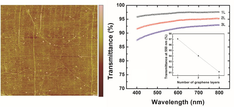
In the past, we have synthesized graphene sheets using Ni thin film (300 nm) as a catalyst layer via atmospheric pressure chemical vapor deposition (APCVD): either single to few-layer graphene sheets or multi-layer graphene sheets (>10 layers). The sheet resistance and optical transmittance obtained from the multi-layer graphene were around 500~1000Ω/sq and 75%, respectively. We further improved the synthesis conditions using copper foil (25 µm) as metal catalyst via low-pressure chemical vapor deposition (LPCVD). This method enabled us to synthesize large area, uniform monolayer graphene (>90%) with improved electrical conductivity (400~500Ω/sq) and optical transmittance (~97%). By transferring several times, we could further improve the quality of graphene electrodes (e.g., 3-layer graphene sheet: 300-400 Ω/sq with >90% transmittance) (Figure 1). We then successfully integrated these graphene sheets into the OPV with overall performance comparable, but slightly inferior, to ITO counterparts, possibly due to the relatively higher sheet resistance. Moreover, due to the hydrophobicity of graphene’s surface, uniform coverage of PEDOT:PSS layer was challenging, which was detrimental to device success rates. Various PEDOT:PSS alternatives were investigated, and it was found that AuCl3 doping significantly improves the graphene OPV device performances, possibly due to the improved conductivity and the work function tuning of graphene electrodes as well as the PEDOT wettability (Figure 2).
-

- Figure 1: (a) Morphology of monolayer graphene transferred onto quartz substrate (AFM image). AFM scan size and height bar are 5×5 µm2 and 10 nm, respectively. (b) Transmittance of graphene sheets of 1 to 3 layers. As-grown LPCVD-synthesized graphene films are mostly single- layered and each additional layer contributes approximately 2.3% opacity over the range of wavelength. Inset indicates the transmittance at 550 nm as a function of the number of the graphene layers.
-
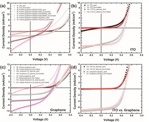
- Figure 2: J-V characteristics of organic solar cells with different anodes under dark and simulated AM1.5G illumination at 100 mW/cm2. Device performances of various types: (a) different PEDOT layer processing (b) ITO and (c) graphene electrodes are demonstrated. Shown in (d) is the comparison of performances of ITO with modified PEDOT:PSS by O2 plasma and graphene doped with AuCl3 (10mM).
- C. W. Tang, “2-layer organic photovoltaic cell,” Applied Physics Letters, vol. 48, pp. 183-185, Jan. 1986. [↩]
- P. Peumans, A. Yakimov, and S. R. Forrest, “Small molecular weight organic thin-film photodetectors and solar cells,” Journal of Applied Physics, vol. 93, pp. 3693-3723, 2003. [↩]
- A. R. Schlatmann, D. W. Floet, A. Hilberer, F. Garten, P. J. M. Smulders, T. M. Klapwijk, and G. Hadziioannou, “Indium contamination from the indium-tin-oxide electrode in polymer light-emitting diodes,” Applied Physics Letters, vol. 69, pp. 1764-1766, Sep. 1996. [↩]
- Z. Chen, B. Cotterell, W. Wang, E. Guenther, and S. J. Chua, “A mechanical assessment of flexible optoelectronic devices,” Thin Solid Films, vol. 394, pp. 202-206, Aug. 2001. [↩]
