Design and Demonstration of Integrated Micro-electro-mechanical (MEM) Relay Power Gating
- Category: Circuits & Systems
- Tags: Hossein Fariborzi, Vladimir Stojanovic
Power gating has become ubiquitous in ICs to reduce the power consumed by inactive CMOS logic circuits. However, the finite Ion/Ioff ratio of MOSFET power gates limits their ability to reduce off-state leakage. In contrast, as described in [1] [2] , micro-electro-mechanical- (MEMS-) based power gates that mechanically make or break electrical contact can completely eliminate off-state leakage (Figure 1). The leakage benefits of MEMS-based power gates may be outweighed by increased switching energy and voltage droop due to relatively large device dimensions and/or operating voltages and on-state resistance. A simple analysis is presented to predict the conditions under which electrostatically-actuated MEM relays can achieve energy savings over MOSFETs for power gates [3] . This analysis shows that even in their current state of technology (~100-μm device pitch), MEM relays can provide energy-reduction benefits over MOSFET power gates for off-periods > 500 μs. With relays scaled to current mass-produced MEMS device dimensions (~ 20 μm), the minimum off-period for energy-reduction benefit reduces to 10 µs.
Relay reliability is improved by the use of hard metals, which results in relatively high contact resistance. For a given relay size, this resistance limits the current density that an array of relay power gates can deliver while maintaining the optimal voltage drop. Current relays can deliver up to ~1 mA/mm2 current density. However, power gates built from moderately scaled relays would support > 10-100 mA/mm2 and would still fit into the same area as the CMOS chip they are driving. The relays could therefore be post-fabricated on top of the chip or integrated into the backend metallization layers with no penalty in the overall die area.
To experimentally demonstrate the feasibility of power-gating with current relay technology, we applied MEM relay power gating to a 90-nm CMOS chip operating at VDD = 0.6-1 V (Ion = 10-25 µA). Figure 2 illustrates the waveforms of the MEM relay power-gating this chip with MEM gate voltages VG swinging between 5 and 7 V, with the inset indicating the chip’s correct I/O activity during Ton.
-
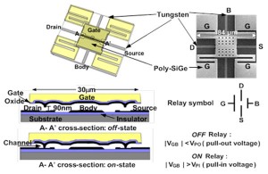
- Figure 1: SEM, diagram, and operating states of the MEM relay device.

-
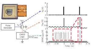
- Figure 2: Schematic and measured waveforms for MEM relay-gated CMOS chip.

- H. Kam, T.K. Liu, E. Alon, M. Horowitz “Circuit level requirements for MOSFET replacement devices,” in IEDM Tech. Dig. 2008. [↩]
- F. Chen, M. Spencer, R. Nathanael, C. Wang, H. Fariborzi, A. Gupta, H. Kam, V. Pott, J. Jeon, T.K. Liu, D. Markovic, V. Stojanovic, E. Alon “Demonstration of integrated micro-electro-mechanical switch circuits for VLSI applications,” in International Solid-State Circuits Conference (ISSCC Tech. Dig.), pp. 150-151, Feb. 2010. [↩]
- H. Fariborzi, M. Spencer, V. Karkare, J. Jeon, R. Nathanael, C. Wang, F. Chen, H. Kam, V. Pott, T.K. Liu, E. Alon, V. Stojanovic, D. Markovic, “Analysis and demonstration of MEM-relay power gating,” in IEEE Custom Integrated Circuits Conference (CICC), 2010 [↩]