A Low-power SAR ADC with Redundancy
- Category: Circuits & Systems
- Tags: Albert Chang, Duane Boning, Hae-Seung Lee
Technology scaling has enabled low-power operations in digital integrated circuits. Therefore, the trend to move analog-to-digital operations upstream to allow more signal-processing to shift from the analog domain to the digital domain is inevitable. As most real world signals remain analog, the design of high-performance and low-power analog-digital converters (ADCs) plays a key role to the success of future integrated system design. In this research, we focus on designing (1) robust, (2) low-power, and (3) high-performance time-interleaved successive-approximation-registers (SAR) ADCs. The SAR architecture is adopted because of its good digital compatibility and high energy-efficiency while achieving high sampling rates.
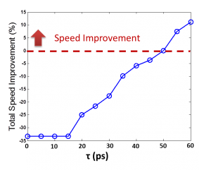
The robustness of SAR ADCs is achieved by analyzing the effectiveness of redundancy (digital error correction) [1] [2] in improving sampling rates and its immunity from incomplete bit settling errors. Analysis shows that the redundancy algorithm does not help improve sampling rate in all SAR ADC designs; instead, the maximum sampling rate depends on the settling time constant (τ) and the relative magnitude of the ADC delay components [3] . As shown in Figure 1, in order to benefit from the redundancy algorithm, τ has to be more than 50 ps.
The low-power operation is achieved by combining the merged capacitor switching algorithm [4] and split capacitive array [5] . The merged capacitor switching algorithm suffers from its sensitivity to the parasitic capacitance on the outputs of the capacitive DAC. The split capacitive array suffers from a 4x loss in signal power to keep voltage below the supply rail on the sub-DAC and the mismatch problem between the fractional bridge capacitor to other capacitors in the DAC. Our design researches and resolves both issues. Our design also incorporated asynchronous on-chip pulse generator to avoid synchronous high power clock distribution circuit on-chip. The overall SAR ADCs architecture is depicted in Figure 2.
- Figure 1: Speed improvement from adopting redundancy [2] .
- Figure 2: Overall SAR ADCs architectures.
- F. Futtner, “A 1.2V 10b 20MSample/s non-binary successive approximation ADC in 0.13μm CMOS,” in IEEE International of Solid-State Circuit Conference Digest of Technical Papers, pp. 136-137, 2002. [↩]
- T. Ogawa, H. Kobayashi, M. Hotta, Y. Takahashi, H. San, and N. Takai, “SAR ADC algorithm with redundancy,” in IEEE APCCAS, pp. 268-271, Nov. 2008. [↩] [↩]
- A. H. Chang, H.-S. Lee, and D. S. Boning, “Redundancy in SAR ADCs,” in Great Lakes Symposium on VLSI, May 2011. [↩]
- V. Hariprasath, J. Guerber, S.-H. Lee, and U.-K. Moon, “Merged capacitor switching based SAR ADC with highest switching energy-efficiency,” Electronics Letters, vol. 46, pp. 620-621, April 2010. [↩]
- Y. Chen, X. Zhu, H. Tamura, M. Kibune, Y. Tomita, T. Hamada, M. Yoshioka, K. Ishikawa, T. Takayama, J. Ogawa, S. Tsukamoto, and T. Kuroda, “Split capacitor DAC mismatch calibration in successive approximation ADC,” in IEEE Custom Integrated Circuits Conference, pp. 279 –282, 2009. [↩]

