A. Wang, B. Yaglioglu, H. Tang, C.G. Sodini, V. Bulović, A.I. Akinwande
Sponsorship: Hewlett-Packard, DARPA
Recently, sputtered metal-oxide-based field-effect transistors (FETs) have
been demonstrated with higher charge carrier mobilities, higher current densities,
and faster response performance than amorphous silicon FETs, which are the
dominant technology used in display backplanes [1-3]. Because the optically
transparent semiconducting oxide films can be deposited at near-room temperatures,
these materials are compatible with future generations of large-area electronics
technologies that require flexible substrates [4]. It is possible to process
FETs by shadow-mask patterning, but this method limits the range of feature
sizes, accuracy of pattern alignment, and scalability of the process to large
substrates. Consequently, our project aims to develop a low-temperature, lithographic
process for metal oxide-based FETs that can be integrated into large-area electronic
circuits.
We have fabricated top-gate, fully lithographic FETs of varying channel lengths
on 100-mm glass wafers with a sputtered ZnO:In2O3 channel layer, using an organic
polymer, parylene, as the gate dielectric and indium-tin-oxide (ITO) for source/drain
contacts. All layers were subtractively patterned by a combination of dry- and
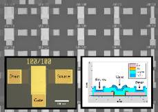
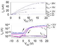
wet-etch processes. Figure 1 shows a micrograph of several completed FETs. Current-voltage
characteristics for a single device (pictured in inset of Figure 1) appear in
Figure 2. From the current-voltage and capacitance-voltage curves, device- and
circuit parameters such as threshold voltage, subthreshold slope, gate leakage,
and channel capacitance can be extracted and also used to monitor the reproducibility
of our process. These measurements are used as a guide to determine processing
conditions for the fabrication of oxide-based field-effect transistors and circuits.
|
|
Figure 1: Micrograph of fabricated array of single devices with varying channel lengths. The left inset gives a larger view of a single field effect transistor (W/L = 100µm / 100µm). The right inset shows a schematic cross-section of the device. |
Figure 2: Electrical characteristics of lithographically patterned FET (W/L = 100µm / 100µm). Output curves are plotted in the top graph; double-swept transfer curves taken in saturation and triode regions are plotted on the bottom. As the bottom graph shows, gate leakage current through the parylene dielectric is low. |
References
L.F. Velásquez-García, A.I. Akinwande
Sponsorship: DARPA
Mass spectrometers need to ionize the sample that they are analyzing to determine
its chemical composition. Traditional ionizers for gases use either chemical
ionization (CI) or electron impact ionization (EII). In the latter case, electrons
from thermionic sources produce ions by colliding with neutral molecules. More
efficient carbon nanotube-based field-emitted electron impact ionizers have been
developed [1]. However, one of the drawbacks of EII is that the sample is transformed
into small fragmentation products. Several samples could have similar fragmentation
spectra but be quite different compounds, with radically different properties.
(For example, one substance can be a poisonous agent while another is a harmless
material). Therefore, an approach to reduce the fragmentation products would
improve the informational power of the mass spectrometer.
Field ionization soft-ionizes molecules, thus reducing the fragmentation products.
The field ionization scheme creates ions by directly tunneling electrons from
the outer shell of neutral molecules by virtue of a very high electric field
[2]. The electric field is produced by high-aspect-ratio field enhancers and
the application of a large (up to 1 kV) bias voltage. Carbon nanotubes (CNTs)
are ideal field enhancers because of their high aspect ratio and their nanometer-sized
tip radius. In the case of the EIIs, a closed architecture is implemented because
it is intended to protect the field enhancers from back-streaming positive ions
[3]. However, this protection is not needed in a field ionizer because in this
case the field enhancers are biased at a positive voltage with respect to the
gate. Also, an open architecture, where the field enhancers are accessible by
the neutral molecules from all directions, is a more suitable approach to produce
field ionization because it increases the ion current. We have implemented the
emitting substrate of an open architecture single-gated field ionizer array [4].
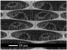
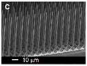
The substrate is a micro-fabricated 3D foam-like silicon structure (µfoam). The
µfoam is fabricated using deep reactive ion-etching (DRIE). On top of the µfoam,
there is a sparse array of plasma-enhanced chemical-vapor-deposited (PECVD) CNTs
(Figure 1) that act as field enhancers. The CNTs are sparsely grown to avoid
field enhancer shadowing. The substrate has been tested with a triode setup.
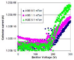
The data shows a startup ionization voltage as low as 175 V (Figure 2). Current
research efforts focus on developing a gated version of the ionizer.
 |
|
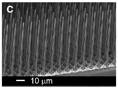
Figure 1: Detail of sparse PECVD CNT cluster on the mfoam. The CNTs have 80-nm-diameter tips and are up to 14 mm tall. |
Figure 2: The IV characteristics of the field ionizer. The collector is a smooth ball of 2 mm diameter hovering about 4 mm above the gate. The collector was biased at –1100 V. The gate is biased at 0 V. |
References
L.F. Velasquez-Garcia, D. Akinwande (Stanford), P. Wong (Stanford), A.I.
Akinwande
Sponsorship: DARPA
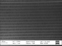
Carbon nanotubes (CNTs) are currently massively investigated due to their remarkable mechanical, thermal, chemical, and electrical properties [1]. CNTs are seamless graphite tubes that can be grown using diverse methods such as arc deposition, chemical vapor deposition (CVD), and plasma-enhanced chemical-vapor-deposition (PECVD) [2]. The best performance comes from CNTs made of a single graphite sheet, i.e., single-walled carbon nanotubes (SWNTs). SWNTs are 1 – 2 nm in diameter and can have lengths over several centimeters [3]. Both in-plane and out-of-plane SWNTs are useful in the device industry. In-plane SWNTs can be used as the channel in transistors, while out-of-plane SWNTs can be used in circuit vias. We are currently investigating the growth of CVD SWNTs using our PECVD reactor. A forest of in-plane SWNTs can be grown using a methane/hydrogen chemistry at 200 Torr and 880°C if 2 Å Fe is used as a catalyst on top of quartz substrates (Figure 1). Sparse forests can be formed at lower pressures and temperatures (Figure 2). Current research focuses on investigating the growth space for in-plane SWNTs and developing growth recipes for out-of-plane SWNTs. With this information, devices will be designed and implemented.
 |
|
Figure 1: A forest of in-plane SWNTs grown at 880ºC and 200 Torr if iron is used as catalyst with a hydrogen/methane mix. The substrate is quartz. |
Figure 2: Sparse growth of in-plane SWNTs occurs if iron is used as a catalyst in a hydrogen/methane mix at 825ºC and 100 Torr. The substrate is quartz. |
References
L.F. Velásquez-García, Y. Niu, A.I. Akinwande
Sponsorship: DARPA, AFOSR
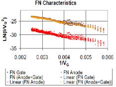
Electrons are field-emitted from the surface of metals and semiconductors when the potential barrier (work function) that holds electrons within the metal or semiconductor is deformed by the application of a high electrostatic field. Field emitters use high-aspect-ratio structures with tips that have nanometer dimensions to produce a high electrostatic field with a low applied voltage. Small changes in the tip radius result in huge changes in the current density because of the exponential dependence of the emitted current on the bias voltage, as described by the Fowler-Nordheim theory. Also, tip radii variation in an array results in non-uniform turn-on voltages. If the emitters are ballasted, the spatial non-uniformity can then be substantially decreased. Furthermore, ballasting individual emitters prevents destructive emission from the sharper tips, resulting in higher overall current emission because of the inclusion of duller tips. Ballasting also results in more reliable operation. The use of large resistors in series with the field emitters is an unattractive ballasting approach because of the resulting low emission currents and power dissipation in the resistors. A better approach for ballasting field emitters is the use of ungated field-effect transistors (FETs) that effectively provide high dynamic resistance with large saturation currents [1]. In the past our research group demonstrated the use of a MOSFET to ballast the emission of electrons from silicon tips [2]. We have implemented a large and dense array of plasma-enhanced chemical-vapor-deposited (PECVD) carbon nanotubes (CNTs) (1-million elements in 1 cm2), in which each emitter is individually ballasted by a high-aspect-ratio column that acts as an ungated FET (Figure 1) [3]. For an n-Si substrate with a high-enough doping level, the Fowler- Nordheim (FN) plot of the data shows no saturation (Figure 2). Current research focuses in systematically studying the dependence of the ballasting on the doping level, showing current limiting data using CNT FEAs, and implementing a gated version of the field-emitter array.
|
|
Figure 1: A PECVD CNT on top of a high-aspect-ratio Si column that acts as an ungated FET to limit the emitter current (A). The CNT is about 4 mm tall and it has 37-nm diameter (B). The FETs are 100 mm tall and have less than 1 mm ´ 1 mm cross-section (C). |
Figure 2: Fowler-Nordheim plot for a 106 CNT emitter array that uses an n-Si substrate with doping level equal to 1´1015 cm-3. The FN model describes the electron current of the device because the doping level of its FETs is not low enough to produce current limitation. |
References
L.F. Velásquez-García, Y. Niu, A.I. Akinwande
Sponsorship: DARPA, AFOSR
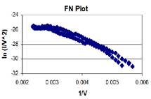
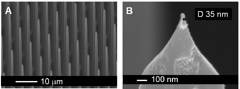
Electrons are field-emitted from the surface of metals and semiconductors when the potential barrier (work function) that holds electrons within the metal or semiconductor is deformed by the application of a high electrostatic field. Field emitters use high- aspect-ratio structures with tips that have nanometer dimensions to produce a high electrostatic field with a low applied voltage. Small changes in the tip radius result in huge changes in the current density because of the exponential dependence of the emitted current on the bias voltage, as described by the Fowler-Nordheim theory. Also, tip radii variation in an array results in non-uniform turn-on voltages. If the emitters are ballasted, the spatial non-uniformity can then be substantially decreased. Furthermore, ballasting individual emitters prevents destructive emission from the sharper tips, resulting in higher overall current emission because of the inclusion of duller tips. Ballasting also results in more reliable operation. The use of large resistors in series with the field emitters is an unattractive ballasting approach because of the resulting low emission currents and power dissipation in the resistors. A better approach for ballasting field emitters is the use of ungated field-effect transistors (FETs) that effectively provide high dynamic resistance with large saturation currents [1]. In the past our research group demonstrated the use of a MOSFET to ballast the emission of electrons from silicon tips [2]. We have implemented a large and dense array of conical Si tips (1 million elements in 1 cm2), where each emitter is individually ballasted by a high-aspect-ratio column that acts as an ungated FET (Figure 1) [3]. The Fowler- Nordheim (FN) plot of the data for lowly doped arrays shows that the ungated FETs limit the emitter current because the slope of the curve becomes horizontal for high-enough current levels (Figure 2). We have obtained electron currents as large as 10 mA, the largest field-emitted currents reported from Si tips. Current research focuses on systematically studying the dependence of the ballasting on the doping level and implementing a gated version of the array.
  |
|
Figure 1: An array of silicon field emitters individually ballasted by vertical ungated FETs (A). The field emitter diameter is about 35 nm (B). The FETs are 100 mm tall and have a less than 1 mm ´ 1 mm cross-section (C). |
Figure 2: Fowler-Nordheim plot for a 4000 Si emitter array that uses an n-Si substrate with doping level equal to 2´1013 cm-3 For unballasted field emitters, the curve is a straight line. The current is limited to the point that the curve becomes horizontal for high enough voltages. |
References
K. Cheung, L.F. Velasquez-Garcia, A.I. Akinwande
Sponsorship: DARPA
In recent years, there has been a desire to scale down linear quadrupoles.
The key advantages of this miniaturization are the portability it enables and
the reduction of pump power needed due to the relaxation on operational pressure.
Attempts at making microelectromechanical systems-based linear quadrupoles
met with varying degrees of success [1-3]. Producing these devices involved
some combination of precision machining or microfabrication and downstream
assembly. For miniature quadrupole mass filters to be mass-produced cheaply
and efficiently, manual assembly should be removed from the process.
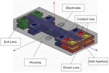
A purely microfabricated quadrupole mass filter consisting of a planar design
and a rectangular electrode geometry has been made. Rectangular rods were utilized
since they are most amenably shaped for planar microfabrication. This deviation
from the conventional round rod geometry required optimization and analysis.
After we minimized unwanted effects through various simulations, we proposed
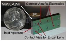
a design (Figure 1), conceived a process flow, and fabricated the Micro-Square
Electrode Quadrupole Mass Filter (MuSE-QMF) (Figure 2). The process requires
the bonding of five silicon wafers and the use of deep reactive ion etching
to pattern the features. It is a relatively simple process, furthering the
case for mass-production of these devices.
This non-conventional design will introduce non-linear resonances that manifest
as peak splitting in the mass spectrum. Reported work involving linear quadrupoles
operated in the second stability region shows improved peak shape without these
splits [3]. It is believed that operating this device in the second stability
region will provide a means to overcome the nonlinear resonances introduced
by the square electrode geometry. Successful implementation of this device
will lead into arrayed configurations for parallel analysis and aligned quadrupoles
operated in tandem for enhanced resolution.
 |
|
Figure 1: Schematic of proposed device. |
Figure 2: Fabricated device. |
References
 Microsystems Technology Laboratories Building 39, Room 553A
60 Vassar Street Cambridge,
MA 02139
Microsystems Technology Laboratories Building 39, Room 553A
60 Vassar Street Cambridge,
MA 02139
P: 617.258.7974 F: 617.253.0062 www.mtl.mit.edu
Copyright © 2008 Massachusetts Institute of Technology
Click here for information on MIT Accessibility.