As MOSFET dimensions are reduced to the sub-micron level, the electrical performance and characteristics are critically dependent on the two- and three-dimensional distribution of dopant concentrations in the semiconductor. Consequently, it has become essential to accurately characterize, predict, and control the diffusion characteristics of dopants during device fabrication.
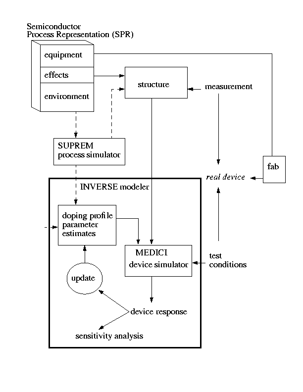
The characterization of dopant distribution in the device is carried out through the use of an inverse modeling technique. Combining numerical optimization techniques with process and device simulation tools, through a careful choice of physical experiments, one is able to extract information of the process as well as device structures that are otherwise impossible or difficult to obtain through direct measurements. Using the super-steep retrograde devices fabricated at MIT as the starting point, we have been able to extract the one-dimensional dopant distribution, as well as some preliminary diffusion characteristics of indium, about which very little information is available in the literature. Experiments to obtain more complete and accurate information on the diffusion characteristics of indium are underway.
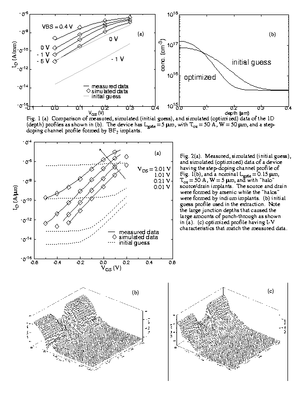
Inverse modeling techniques for obtaining channel doping profiles from device electrical measurements have been investigated. Constant current threshold voltage measurements and capacitance measurements were made on NMOS long channel devices and long channel super steep retrograde doped NMOS devices. Different representations of profiles were explored and simulation results obtained using these profiles were then converged to the output measurements using optimization algorithms. The best results were obtained using an optimizer which relies on a Levenberg Marquardt algorithm for profile variation.
On-going work involves the development of an accurate two-dimensional characterization technique that allows one to calibrate and subsequently predict with high accuracy the electrical characteristics of MOSFETs.
Publications
Rahman, N. E. Extraction of MOSFET Doping Profiles from Device Electrical Measurements. M. Eng. Thesis. Dept. of Electr. Eng. and Comput. Sci., MIT, 1996.
Lee, Z., D. Antoniadis, and M. McIlrath, in Proceedings of the 1997 International Electron Devices Meeting(IEDM), Washington, D.C., December, 1997.