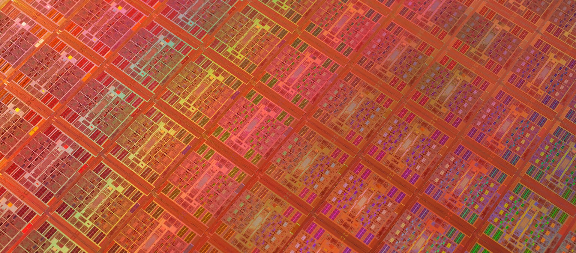
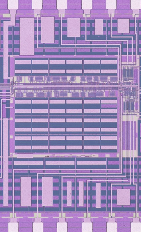
Chip and System Gallery
A Threshold-Based Bioluminescence Detector with a CMOS-Integrated Photodiode Array in 65 nm for a Multi-Diagnostic Ingestible Capsule
Qijun Liu
March 2023
This article presents a highly miniaturized ingestible electronic capsule for biochemical detection via onboard genetically engineered biosensor bacteria. The core integrated circuit (IC) is a threshold-based bioluminescence detector with a CMOS-integrated photodiode array in a 65-nm technology that utilizes a dual-duty-cycling front end to achieve low power consumption. The implemented IC achieved 59-nW active power consumption, 25-fA/count resolution, and a 59-fA minimum detectable signal (MDS) using a calibrated optical source. The IC was then integrated with other system components into a battery-powered wireless ingestible capsule measuring just 6.5 mm thick x 12 mm diameter. We demonstrated successful detection of low-intensity bioluminescent signals from bioengineered bacterial sensors when exposed to the intestinal inflammation biomarker tetrathionate in vitro. Together, the IC and mm-scale smart pill systems demonstrate high sensitivity with low-power multiplexed measurement capability suitable for noninvasive disease diagnosis and monitoring in the gastrointestinal (GI) tract.
Batteryless, Wireless, and Secure SoC for Implantable Strain Sensing
Mohamed R. Abdelhamid
December 2022
The past few years have witnessed a growing interest in wireless and batteryless implants, due to their potential in long-term biomedical monitoring of in-body conditions such as internal organ movements, bladder pressure, and gastrointestinal health. Early proposals for batteryless implants relied on inductive near-field coupling and ultrasound harvesting, which require direct contact between the external power source and the human body. To overcome this near-field challenge, recent research has investigated the use of RF backscatter in wireless micro-implants because of its ability to communicate with wireless receivers that are placed at a distance outside the body (∼0.5 m), allowing a more seamless user experience. Unfortunately, existing far-field backscatter designs remain limited in their functionality: they cannot perform biometric sensing or secure data transmission; they also suffer from degraded harvesting efficiency and backscatter range due to the impact of variations in the surrounding tissues. In this paper, we present the design of a batteryless, wireless and secure system-on-chip (SoC) implant for in-body strain sensing. The SoC relies on four features: 1) employing a reconfigurable in-body rectenna which can operate across tissues adapting its backscatter bandwidth and center frequency; 2) designing an energy efficient 1.37 mmHg strain sensing front-end with an efficiency of 5.9 mmHg·nJ/conversion; 3) incorporating an AES-GCM security engine to ensure the authenticity and confidentiality of sensed data while sharing the ADC with the sensor interface for an area efficient random number generation; 4) implementing an over-the-air closed-loop wireless programming scheme to reprogram the RF front-end to adapt for surrounding tissues and the sensor front-end to achieve faster settling times below 2 s.
A ThreshoId-ImpIementation-Based Neural-Network Accelerator Securing Model Parameters and Inputs Against Power Side-Channel Attacks
Saurav Maji
November 2022
With the recent advancements in machine learning (ML) theory, a lot of energy-efficient neural network (NN) accelerators have been developed. However, their associated side- channel security vulnerabilities pose a major concern. There have been several proof-of-concept attacks demonstrating the extraction of their model parameters and input data. This work introduces a threshold implementation (TI) masking-based NN accelerator that secures model parameters and inputs against power and electromagnetic (EM) side-channel attacks. The 0.159 mm2 demonstration in 28 nm runs at 125 MHz at 0.95 V and limits the area and energy overhead to 64% and 5.5×, respectively, while demonstrating security even greater than 2M traces. The accelerator also secures model parameters through encryption and the inputs against horizontal power analysis (HPA) attacks.
A Bit-level Sparsity-aware SAR ADC with Direct Hybrid Encoding for Signed Expressions for AIoT Applications
Ruicong Chen
August 2022
In this work, we propose the first bit-level sparsity-aware SAR ADC with direct hybrid encoding for signed expressions (HESE) for AIoT applications. ADCs are typically a bottleneck in reducing the energy consumption of analog neural networks (ANNs). For a pre-trained Convolutional Neural Network (CNN) inference, a HESE SAR for an ANN can reduce the number of non-zero signed digit terms to be output, and thus enables a reduction in energy along with the term quantization (TQ). The proposed SAR ADC directly produces the HESE signed-digit representation (SDR) using two thresholds per cycle for 2-bit look-ahead (LA). A prototype in 65nm shows that the HESE SAR provides sparsity encoding with a Walden FoM of 15.2fJ/conv.-step at 45MS/s. The core area is 0.072mm2.
A Dual-Antenna, 263-GHz Energy Harvester in CMOS for Ultra-Miniaturized Platforms with 13.6% RF-to-DC Conversion Efficiency at −8 dBm Input Power
Muhammad Ibrahim Wasiq Khan
June 2022
This paper reports a CMOS energy harvester, which operates at so far the highest reported frequency (263 GHz) in order to realize wireless powering of ultra-miniaturized platforms. To maximize the THz-to-DC conversion efficiency, n, at low available radiation power, the harvester not only utilizes a high-speed 22-nm FinFET transistor but also achieves the optimal operating conditions of the device. In specific, the circuit enables self-gate biasing; and through a dual-antenna topology, it drives the transistor drain and gate terminals with both optimal voltage phase difference and power ratio simultaneously and precisely. With a low input power of −8 dBm, the harvester achieves 13.6% measured conversion efficiency and delivers 22 µW to a 1-kΩ load. Without relying on any external component, the harvester chip occupies an area of 0.61 * 0.93 mm2.
RaM-SAR: A Low Energy and Area Overhead, 11.3 fJ/conv.-step 12b 25MS/s Secure Random-Mapping SAR ADC with Power and EM Side-channel Attack Resilience
Ruicong Chen
June 2022
This paper presents RaM-SAR, a 12b 25MS/s 11.3fJ/conv.-step secure random-mapping SAR ADC with power and EM side-channel attack resilience. Each conversion is randomly mapped to one of the thousands of conversion sequences to randomize power supply traces. This technique protects against neural network based power and EM side-channel attacks. It enables protection with much lower energy and area overheads compared to the prior works. A prototype in 65nm CMOS demonstrates significant improvements with 12.5× higher bandwidth and 4.8× better energy-efficiency over prior works.
Randomized Switching SAR (RS-SAR) ADC Protections for Power and Electromagnetic Side Channel Security
Maitreyi Ashok
October 2022
Analog to digital converters (ADCs) are necessary in most Internet of Things (loT) devices, to link the physical analog world to digital computation. Physical side channel attacks (SCAs) have been used to reconstruct information processed within digital integrated circuits in a variety of applications, through power or electromagnetic (EM) traces [1]. Furthermore, power SCAs have successfully decoded the analog information converted within Successive Approximation Register (SAR) ADCs [2], [3]. Previous works have proposed initial protections, such as switched-capacitor current equalization for power SCAs [2], random dithering for the reference charge [3], or general power side channel security using a stacked digital low dropout array and random noise injection [4]. Whereas power SCAs require cutting the power trace and introducing a shunt resistor for measurement, EM SCAs can effectively perform non-invasive measurements external to packaging (Fig. 1). However, supply current equalization is not effective against localized EM SCAs, which can probe currents directly above the ADC circuitry.
A Threshold Implementation-Based Neural Network Accelerator With Power and Electromagnetic Side-Channel Countermeasures
Saurav Maji
February 2022
With the recent advancements in machine learning (ML) theory, a lot of energy-efficient neural network (NN) accelerators have been developed. However, their associated side-channel security vulnerabilities pose a major concern. There have been several proof-of-concept attacks demonstrating the extraction of their model parameters and input data. This work introduces a threshold implementation (TI) masking-based NN accelerator that secures model parameters and inputs against power and electromagnetic (EM) side-channel attacks. The 0.159 mm 2 demonstration in 28 nm runs at 125 MHz at 0.95 V and limits the area and energy overhead to 64% and 5.5 × , respectively, while demonstrating security even greater than 2M traces. The accelerator also secures model parameters through encryption and the inputs against horizontal power analysis (HPA) attacks.
A 0.31THz CMOS Uniform Circular Antenna Array Enabling Generation/Detection of Waves with Orbital-Angular Momentum
Muhammad Ibrahim Wasiq Khan
June 2021
This paper reports the first chip-based demonstration (at any frequency) of a CMOS front-end that generates and receives electromagnetic waves with rotating wave phase front (namely orbital angular momentum or OAM). The chip, based on a uniform circularly placed patch antenna array at 0.31THz, transmits reconfigurable OAM modes, which are digitally switched among the m=0 (plane wave), +1 (left-handed), -1 (right-handed) and superposition (+1)+(-1) states. The chip is also reconfigurable into a receiver mode that identifies different OAM modes with >10dB rejection of unintended modes. The array, driven by only one active path, has a measured EIRP of -4.8dBm and consumes 154mW of DC power in the OAM source mode. In the receiver mode, it has a measured conversion loss of 30dB and consumes 166mW of DC power. The output OAM beam profiles and mode orthogonality are experimentally verified and a full silicon OAM link is demonstrated.
A Low-Power Elliptic Curve Pairing Crypto-Processor for Secure Embedded Blockchain and Functional Encryption
Utsav Banerjee
April 2021
Our pairing hardware implementation enables more than two orders of magnitude improvement in performance and energy-efficiency compared to embedded software. Several circuit, architecture and algorithm techniques are used to achieve this energy-efficient design. A 64-bit word-serial Montgomery modular arithmetic unit provides up to 50% energy savings compared to traditional designs with smaller word sizes. Karatsuba-style divide-and-conquer techniques are used to reduce energy consumption of the pairing computation by 35%. Strategically sharing computations between the Miller Loop and the Final Exponentiation gives another 30% energy savings. A hierarchical memory architecture with dedicated clock gates is used to achieve additional 20% reduction in energy consumption. Special properties of the BLS12-381 curve are exploited to further provide up to 2x improvement in performance and energy-efficiency of different pairing-based algorithms
A 770 kS/s Duty-Cycled Integrated-Fluxgate Magnetometer for Contactless Current Sensing
Preetinder Garcha
February 2021
This work describes a sampling-rate scalable, package-integrated magnetometer with CMOS-integrated fluxgate, that achieves 100x lower compensation energy with duty cycling for 1kHz power monitoring applications, while achieving 1.67x higher peak BW than previous IFG sensors for fault detection. Key contributions include 1) mixed signal front-end design to hold digitized compensation value during sleep and resume operation from last converged point (LCP), saving up to 100 convergence cycles when duty cycling, 2) hierarchical bypass/coarse/fine search modes to guarantee quick convergence (< 20μs), even for 2mT field swing between samples in heavily-duty-cycled systems, and 3) faster sampling and read out (1.3μs) for lower energy per sample and higher BW.
S2ADC: A 12-bit, 1.25MS/s Secure SAR ADC with Power Side-Channel Attack Resistance
Taehoon Jeong
March 2020
This work presents a neural-network-based SAR ADC power side-channel attack (PSA) method and a 12-bit, 1.25MS/s secure SAR ADC whose current equalizers protect the ADC from PSA. A prototype SAR ADC was fabricated in 65nm CMOS to demonstrate the proposed concepts. Without PSA protection, the proposed PSA method decoded the power supply current waveforms of the prototype ADC into the corresponding A/D converter output bits with >99% bit-wise accuracy except for the LSB. With PSA protection, the prototype ADC demonstrated high resistance to the proposed PSA method, showing significant drop in bit-wise accuracy.
A Low-Power Dual-Factor Authentication Unit for Secure Implantable Devices
Saurav Maji
March 2020
This work presents a dual-factor authentication protocol and its low-power implementation for security of implantable medical devices (IMDs). The protocol incorporates traditional cryptographic first-factor authentication using Datagram Transport Layer Security - Pre-Shared Key (DTLS-PSK) followed by the user's touch-based voluntary second-factor authentication for enhanced security. With a low-power compact always-on wake-up timer and touch-based wake-up circuitry, our test chip consumes only 735 pW idle state power at 20.15 Hz and 2.5 V. The hardware accelerated dual-factor authentication unit consumes 8 μW at 660 kHz and 0.87 V. Our test chip was coupled with commercial Bluetooth Low Energy (BLE) transceiver, DC-DC converter, touch sensor and coin cell battery to demonstrate standalone implantable operation and also tested using in-vitro measurement setup.
THzID: A 1.6mm2 Package-Less Cryptographic Identification Tag with Backscattering and Beam-Steering at 260GHz
Mohamed I. Ibrahim, Ibrahim W. Khan, Chiraag Juvekar, Wanyeong Jung, Rabia Tugce Yazicigil
February
2020
Energy-autonomous wireless tags have been adopted in authentication and supply-chain management. At present, their size and cost, limited by packaging, prevent the tagging for small or inexpensive industrial/medical components. At the same time, pervasive electronic tagging raises serious privacy concerns related to inadvertent and malicious tracking of the tagged assets. In order to enable secure and ubiquitous asset tagging, fully passive particle-sized cryptographic chips without external packaging are highly desired. Recent prototypes that aim to address this challenge face either size, energy, communication, or security limitations. In this work, we present a package-less, monolithic tag chip with built-in photovoltaic powering and a compact elliptic-curve-cryptography (ECC) processor. Using far-field backscatter communication at 260GHz, the CMOS tag, while integrating a 2×2 antenna array with beam-steering capability, has a size of only 1.6mm2.
An Energy-Efficient Configurable Lattice Cryptography Processor for the Quantum-Secure Internet of Things
Utsav Banerjee
February 2019
Modern public key protocols, such as RSA and elliptic curve cryptography, will be rendered insecure by Shor's algorithm when large-scale quantum computers are built. Therefore, cryptographers are working on quantum-resistant algorithms, and lattice-based cryptography has emerged as a prime candidate. However, high computational complexity of these algorithms makes it challenging to implement lattice-based protocols on resource-constrained IoT devices, which need to secure data against both present and future adversaries. To address this challenge, we present a lattice cryptography processor with configurable parameters, which enables up to two orders of magnitude energy savings and 124K-gate reduction in system area through architectural optimizations. The ASIC demonstrates multiple lattice-based protocols proposed in the NIST post-quantum standardization process.
SHARC: Self-Healing Analog with RRAM and CNFETs
Aya G. Amer
February 2019
Carbon nanotube (CNT) field-effect transistors (CNFETs) are a promising emerging technology for energy-efficient electronics. Despite this promise, CNTs are subject to substantial inherent imperfections; every ensemble of CNTs includes some percentage of metallic CNTs (m-CNTs). m-CNTs result in conductive shorts between CNFET source and drain, resulting in excessive leakage and degraded (potentially incorrect) circuit functionality. Several techniques have been developed to remove the majority of m-CNTs (no technique today removes 100% of m-CNTs). While these techniques enabled the first digital CNFET circuits, it is still not possible to realize large-scale CNFET analog or mixed-signal CNFET circuits due to m-CNTs. While a digital logic gate can still function correctly in the presence of a small fraction of m-CNTs (but with degraded resilience to noise), a single m-CNT in an analog circuit can result in catastrophic failure (e.g., degrading amplifier gain resulting in functional failure of circuit blocks such as ADCs and DACs). This work presents a circuit design technique, Self-Healing Analog with RRAM and CNFETs (SHARC), that leverages the programmability of non-volatile resistive RAM (RRAM) to automatically “self-heal” analog circuits in the presence of m-CNTs. Using SHARC, we experimentally demonstrate analog CNFET circuits robust to m-CNTs as well as the first mixed-signals CNFET sub-system (4-bit DAC and SAR ADC; these are the largest reported complementary (CMOS) CNFET circuit demonstrations to-date).
Ultra-Fast Bit-Level Frequency-Hopping Transmitter for Securing Low-Power Wireless Devices
Rabia Tugce Yazicigil
June 2018
Current BLE transmitters are susceptible to selective jamming due to long dwell times in a channel. To mitigate these attacks, we propose physical-layer security through an ultra-fast bit-level frequency-hopping (FH) scheme by exploiting the frequency agility of bulk acoustic wave resonators (BAW). Here we demonstrate the first integrated bit-level FH transmitter (TX) that hops at 1μs period and uses data-driven random dynamic channel selection to enable secure wireless communications with additional data encryption. This system consists of a time-interleaved BAW-based TX implemented in 65nm CMOS technology with 80MHz coverage in the 2.4GHz ISM band and a measured power consumption of 10.9mW from 1.1V supply.
A −80dBm BLE-Compliant, FSK Wake-Up Receiver with System and Within-Bit Duty-Cycling for Scalable Power and Latency
Mohamed R. Abdelhamid
April 2018
This work presents an FSK wake-up receiver with a -80 dBm sensitivity using a packet structure and a duty cycling scheme compliant with the Bluetooth Low Energy (BLE) protocol trading off power with latency. Event-driven applications achieve power lower than 240nW from a 0.75V supply while latency-critical systems wake up in almost 200μW at a 230μW consumption. A within-bit LC oscillator duty-cycling scheme is proposed to provide an extra 24% power reduction. Additionally, a custom FSK transmitter can trigger wake-up at 17nW only for an average latency of 5 seconds.
A Low-Power Integrated Power Converter for an Electromagnetic Vibration Energy Harvester
Ujwal Radhakrishna
April 2018
This work demonstrates the first fully-functional integrated power converter designed to interface a MEMS-based electromagnetic (EM) vibration energy harvester for near-50 Hz operation. The IC accomplishes (i) cold startup from a 50 Hz-150-mV-peak AC input to a 1.1-V output, (ii) conjugate impedance matching for maximum power extraction along with resonant frequency tuning and (iii) input-AC-to-output-DC voltage conversion. Cold startup is achieved using an on-chip Meissner oscillator with an off-chip transformer. Thereafter, a self-timed current-feedback-based H-bridge circuit is turned on for conjugate impedance matching with on-chip control and an off-chip microcontroller for impedance synthesis. The regular-operation H-bridge circuit delivers 820 uW to a load capacitor at 71% efficiency at resonance. It also performs frequency tuning to deliver 650 uW (57%-efficiency) at 50% off-resonance, thereby demonstrating robustness to possible harvester-resonance variations due to manufacturing tolerances. This makes it the first demonstration of a full-system low-power interface IC for vibrational energy harvesters. The prototype is fabricated in 0.18 um CMOS process with an active area of 1.5 mm2.
An Energy-Efficient Reconfigurable DTLS Cryptographic Engine for End-to-End Security in IoT Applications
Utsav Banerjee
February 2018
End-to-end security protocols, like Datagram Transport Layer Security (DTLS), enable the establishment of mutually authenticated confidential channels between edge nodes and the cloud, even in the presence of untrusted and potentially malicious network infrastructure. While this makes DTLS an ideal solution for IoT, the associated computational cost makes software-only implementations prohibitively expensive for resource-constrained embedded devices. We address this challenge through three key contributions: reconfigurable cryptographic accelerators enable two orders of magnitude energy savings, a dedicated DTLS engine offloads control flow to hardware reducing program code and memory usage by ~10x, and an on-chip RISC-V core exercises the flexibility of the cryptographic accelerators to demonstrate security applications beyond DTLS.
Conv-RAM: An Energy-Efficient SRAM with Embedded Convolution Computation for Low-Power CNN-Based Machine Learning Applications
Avishek Biswas
February 2018
Convolutional neural networks (CNN) provide state-of-the-art results in a wide variety of machine learning (ML) applications, ranging from image classification to speech recognition. However, they are very computationally intensive and require huge amounts of storage. Recent work strived towards reducing the size of the CNNs proposes a binary-weight-network (BWN), where the filter weights are ±1 (with a common scaling factor per filter: α). This leads to a significant reduction in the amount of storage required for the weights, making it possible to store them entirely on-chip. However, in a conventional all-digital implementation, reading the weights and the partial sums from the embedded SRAMs require a lot of data movement per computation, which is energy-hungry. To reduce data-movement, and associated energy, we present an SRAM-embedded convolution architecture, which does not require reading the weights explicitly from the memory. Prior work on embedded ML classifiers have focused on 1b outputs or a small number of output classes, both of which are not sufficient for CNNs. This work uses 7b inputs/outputs, which is sufficient to maintain good accuracy for most of the popular CNNs. The convolution operation is implemented as voltage averaging, since the weights are binary, while the averaging factor (1/N) implements the weight-coefficient α (with a new scaling factor, M, implemented off-chip).
Single-BAW Multi-Channel Transmitter with Low Power and Fast Start-Up Time
Phillip Nadeau, Rabia Tugce Yazicigil
September 2017
This work presents a multi-channel transmitter (TX) architecture that uses only a single bulk acoustic wave (BAW) resonator while covering 88 MHz of bandwidth. The proposed architecture overcomes the limited tuning range of a single BAW resonator by combining the BAW tuning range with a programmable integer-N frequency division and RF single-sideband (SSB) mixing approach. The single-BAW multi-channel TX achieves 88 MHz-wide frequency coverage with 1 MHz channels. It operates in the 2.4 GHz ISM band and the full system is demonstrated with 0 dBm output power and a fast system startup time of 2.3 μs enabled by the BAW resonator. It is implemented in 65 nm CMOS technology in a 2 mm × 2 mm area and consumes 6.4 mW from a 1.1 V supply.
0.3 V Ultra-Low Power Sensor Interface for EMG
Sirma Orguc, Harneet Singh Khurana
September 2017
A low-voltage, ultra-low power sensor interface for electromyogram (EMG) signal acquisition is presented. The sensor interface consists of an amplifier and a SAR ADC that work from a 0.3V supply. The low-voltage amplifier topology provides a noise level of 26μVrms, 40dB gain and a state-of the art power efficiency factor (PEF) of 2.2 from a 20-425Hz bandwidth. Low-voltage supply improves the power efficiency of the amplifier compared with previous ultra-low power work. Together with the ADC, the prototype implemented in 65nm CMOS process consumes 3.8nW and has an area of 0.22mm2, which makes the sensor interface suitable for wearable IoT nodes as well as implantable devices.
A 25 mV-Startup Cold Start System with On-Chip Magnetics for Thermal Energy Harvesting
Preet Garcha
September 2017
Thermal energy harvesting systems use boost converters for high-efficiency low voltage operation, but lack the ability for low voltage startup without off-chip transformers. We present a cold start system that uses integrated magnetics instead of external transformers in a Meissner Oscillator to start up from ultra low voltages, with a switched capacitor DC-DC circuit for additional voltage gain. The oscillator analysis with on-chip magnetics allows device co-optimization for low voltage operation, despite 1000x lower inductance values than off-chip transformers. Co-optimized on-chip transformer and depletion-mode NMOS start up from 25 mV driven directly by a sourcemeter, or 50 mV with a 4.7 Ω series resistance, for the lowest integrated electrical startup. The co-packaged system provides proof of concept for integration with boost converter circuits on a single die to have a fully-integrated low voltage startup solution for thermal energy harvesting applications, without using off-chip transformers.
A Fully-Integrated Energy-Efficient H.265/HEVC Decoder with eDRAM for Wearable Devices
Mehul Tikekar
June 2017
Data movement to and from off-chip memory dominates energy consumption in most video decoders, with DRAM accesses consuming 2.8x-6x more energy than the processing itself. We present a H.265/HEVC video decoder with embedded DRAM (eDRAM) as main memory. We propose the following techniques to optimize data movement and reduce the power consumption of eDRAM: 1) lossless compression is used to store reference frames in 2x fewer eDRAM banks, reducing refresh power by 33%; 2) eDRAM banks are powered up on-demand to further reduce refresh power by 33%; 3) syntax elements are distributed to four decoder cores in a partially compressed form to reduce decoupling buffer power by 4x. These approaches reduce eDRAM power by 2x in a fully-integrated H.265/HEVC decoder with the lowest reported system power. The decoder chip requires no external components and consumes 24.9-30.6mW for 1920×1080 video at 24-50 fps.
An ASIC for Energy-Scalable, Low-Power Digital Ultrasound Beamforming
Bonnie Lam
October 2016
In ultrasound imaging systems, a large number of waveforms are acquired in parallel from a transducer array. To facilitate the move to portable ultrasound systems with real-time displays, we implemented a low-power digital beamformer ASIC in 65 nm bulk CMOS technology. We describe three operating modes that provide a run-time tradeoff between image quality and system power consumption. A sliding window approach eliminates the need for an on-chip SRAM, which reduces area and power. The chip generates four output pixels per clock cycle from eight channel of input data, allowing 30 frames per second at 1.92 MHz. The prototype test chip is operational down to a core supply voltage of 0.49 V, with a measured power of 185 uW in real-time operation at 0.52 V.
A Wireless Power Receiver with Active Detuning for Charger Authentication and Dynamic Power Balancing
Nachiket Desai, Chiraag Juvekar
June 2016
As wireless charging becomes more commonplace for IoT devices, several scale-related issues need to be addressed. This chip implements the capability for a near-field, resonant wireless power receiver to detune itself (i.e. move its resonant frequency away) from the charger without the use of any switched passive component arrays. Detuning can be used to protect the receiver against harmful transients imposed by counterfeit wireless chargers, which are expected to become more prevalent the same way as counterfeit wired chargers are currently. In addition, a receiver can detune itself to allow more power to be delivered to a farther receiver coupled to the same charger.
A Buck Converter with 240pW Quiescent Power, 92% Peak Efficiency and a 2x10⁶ Dynamic Range
Arun Paidimarri
April 2016
A buck converter in 65nm CMOS is optimized for a low quiescent power of 240pW. It operates with input 1.2-3.3V and regulates the output from 0.7-0.9V. Control circuits are designed for low-leakage and static current, and scale in power over a Hz to MHz frequency range, resulting in a wide load current dynamic range of 2E6. With a 2V input, the converter has a peak efficiency of 89% and delivers 500pA to 1mA with efficiency better than 50%. The peak efficiency is 92% for a 1.2V input.
Speech Recognizer and Voice Activity Detector
Michael Price
February 2016
This chip performs automatic speech recognition (ASR) and voice activity detection (VAD). ASR accuracy and memory efficiency are enhanced by the use of compressed neural network acoustic models and a variety of modeling and search techniques, allowing real-time decoding with around 10 MB/s external memory bandwidth. ASR models can be imported after training with open-source tools (Kaldi). We evaluated tasks with vocabulary sizes from 11 words (172 uW) to 145k words (7.78 mW); accuracy is comparable to the equivalent Kaldi software recognizer. VAD is used to enable voice-activated power gating of the ASR and downstream system. We include three VAD algorithms to investigate tradeoffs between performance and power consumption. The modulation frequency algorithm is the most robust to difficult noise environments and consumes 22.3 uW.
Nanowatt Circuit Interface to Whole-Cell Bacterial Sensors
Phillip Nadeau
June 2015
In this work we designed a nanowatt-level readout system for bioluminescence measurements from bacterial cells. The system achieves 600 nJ/conversion from external NPN phototransistors with an effective photon noise flux of 5.3 × 10⁵ ph/mm². The system can successfully detect bioluminescence produced by engineered heavy-metal sensing bacteria using 4.0 × 10⁶ cells in 15 µL of sample.
A Reconfigurable Conditional Pre-Charge 16kbit SRAM in 28nm FD-SOI
Chuhong Duan
June 2015
This work presents a data-dependent SRAM paired with statistical methods to leverage data correlation for the purpose of low power read operations. A 10T bit-cell, a prediction-based conditional pre-charge circuit, and a compact column circuit implemented in a 16kbit 28nm SRAM test chip demonstrate power savings up to 69% for applications spanning signal processing, video coding and computer vision as compared to similar memories with naive prediction.
An Energy-Scalable Accelerator for Blind Image Deblurring
Priyanka Raina
April 2015
Camera shake is the leading cause of blur in cell-phone camera images. Removing blur requires deconvolving the blurred image with a kernel which is typically unknown and needs to be estimated from the blurred image. This kernel estimation is computationally intensive and takes several minutes on a CPU which makes it unsuitable for mobile devices. This work presents the first hardware accelerator for kernel estimation for image deblurring applications. Our approach, using a multi-resolution IRLS deconvolution engine with DFT based matrix multiplication, a high-throughput image correlator and a high-speed selective update based gradient projection solver, achieves a 78x reduction in kernel estimation runtime, and a 56x reduction in total deblurring time for a 1920x1080 image enabling quick feedback to the user. Configurability in kernel size and number of iterations gives up to 10x energy scalability, allowing the system to trade-off runtime with image quality. The test chip, fabricated in 40 nm CMOS, consumes 105 mJ for kernel estimation running at 83 MHz and 0.9 V, making it suitable for integration into mobile devices.
A 0.6V 8mW 3D Vision Processor for a Navigation Device for the Visually Impaired
Dongsuk Jeon
April 2015
3D imaging devices, such as stereo and time-of-flight (ToF) cameras, measure distances to the observed points and generate a depth image where each pixel represents a distance to the corresponding location. The depth image can be converted into a 3D point cloud using simple linear operations. This spatial information provides detailed understanding of the environment and is currently employed in a wide range of applications such as human motion capture. However, its distinct characteristics from conventional color images necessitate different approaches to efficiently extract useful information. This chip is a low-power vision processor for processing such 3D image data. The processor achieves high energy-efficiency through a parallelized reconfigurable architecture and hardware-oriented algorithmic optimizations. The processor will be used as a part of a navigation device for the visually impaired. This handheld or body-worn device is designed to detect safe areas and obstacles and provide feedback to a user. We employ a ToF camera as the main sensor in this system since it has a small form factor and requires relatively low computational complexity.
A Low-Noise Instrumentation Amplifier for Sensors using a Noise-Efficient 0.2V-Supply Input Stage
Frank Yaul
April 2015
In low-bandwidth, low-noise applications of wireless sensor nodes, the sensor front-end amplifier presents a power consumption bottleneck since its current draw is noise-limited and cannot be scaled with the low data rate, as is possible with the DSP and RF blocks. Prior work to improve the energy-efficiency of low-noise instrumentation amplifiers (LNIAs) for sensors includes chopper IAs, inverter-based LNAs, current-reuse through amplifier stacking, and low supply voltage amplifier design reaching 0.45V. This work presents an analog front-end (AFE) that achieves an Power Efficiency Figure (PEF) of 1.6 by using a chopper LNIA with a 0.2V-supply inverter-based input stage followed by a 0.8V-supply folded-cascode common-source (FCCS) stage. The high input-stage current needed to reduce the input-referred noise is drawn from the 0.2V supply, significantly reducing power consumption. The 0.8V stage provides high gain and signal swing, improving linearity.
A 0.36V Energy-Efficient 128Kb 6T SRAM with Output Data Prediction in 28nm FDSOI
Avishek Biswas
February 2015
The aggressive scaling of SRAM bit-cell size with every technology node makes it extremely challenging to reduce the Vdd,min of SRAMs, due to the increasing effect of device variations. However, Vdd scaling is crucial in reducing the energy consumption of SRAMs, which is a significant portion of the overall energy consumption in modern micro-processors. Energy savings in SRAM are particularly important for battery-operated applications, which run from a very constrained power-budget. This work presents a low-voltage, energy-efficient SRAM designed in a 28nm fully depleted SOI (FDSOI) technology. The SRAM achieves a minimum Vdd of 0.36V, while still having the area advantage by using 6T bit-cells. Dynamic forward body-biasing is used to improve the Vdd,min. Improved array layout helps in reducing the switching energy. An average energy/bit-access of 52.5fJ has been achieved at 0.45V. Furthermore, by implementing data prediction in the read-path, up to 36% dynamic energy savings are obtained.
A Keccak-based Wireless Authentication Tag with Per-Query Key Update and Power-Glitch Attack Countermeasures
Chiraag Juvekar, Hyung-Min Lee
February 2015
This chip is a wireless authentication tag for supply chain integrity applications. Since the tags are intended to be used for anti-counterfeiting countermeasures against physical attacks are crucial. The tag implements FeCap based NV-DFFs along with an on-chip energy backup solution. This when combined with a custom key update protocol provides resilience against side-channel and power glitch attacks. The tag also implements a new regulating voltage multiplier topology and pulse position modulation for efficient power and data-transfer over a 433MHz near field inductive link.
A Resonant Receiver with Maximum Efficiency-Tracking for Device-to-Device Wireless Charging
Nachiket Desai
November 2014
The growing number of IoT devices calls for new solutions for efficient power delivery that are also more scalable than wired systems. Energy harvesting in an indoor environment is usually limited in output power, while wireless charging using near-field magnetic coupling requires close proximity between the Tx and Rx. In order to recharge these devices without affecting their operation, this work proposes using portable transmitters by adding wireless charging capability to smartphones, for example. In such a system, maximizing system efficiency throughout the entire charging cycle instead of output power becomes the primary concern. The receiver IC consists of a resonant rectifier implemented using synchronously driven, on-chip switches and off-chip passives that reduces switching losses and lowers switch voltage stress. The system also implements a maximum system efficiency-tracking loop that requires no explicit communication with the Tx. The receiver IC includes analog sense circuitry for the tracking loop and a boost regulator at the output of the rectifier. The analog measurements are digitized by an off-chip microcontroller, which calculates the efficiency and moves the operating point of the system towards the maximum efficiency-point by changing the duty cycle input of the boost regulator.
A Vertical Solenoid Inductor for Noise Coupling Minimization in 3D-IC
Gilad Yahalom
July 2014
This chip presents the use of an integrated solenoid inductor in three dimensional integrated circuits (3D-IC) for improved noise mitigation. The structure is fabricated in a two-tier, stacked 28nm CMOS using through silicon vias (TSV). The structure is implemented as part of an LC voltage-controlled oscillator (VCO), and exhibits 6dB improvement in phase noise and 14dB less coupling from adjacent digital clock lines compared to a planar two-turn inductor.
Solar Energy Harvesting System with Integrated Battery Management and Startup Using Single Inductor and 3.2nW Quiescent Power
Dina El-Damak
June 2014
A solar energy harvesting chip with 3.2nW quiescent power. The chip integrates self-startup, battery management, supplies 1V regulated rail with single inductor and supports power range of 10nW to 1μW. The control circuit is designed in an asynchronous fashion that scales the effective switching frequency of the converter with the level of the power transferred. The on-time of the converter switches adapts dynamically to the input and output voltages for peak-current control and zero-current switching. For input power of 500nW, the proposed system achieves an efficiency of 82%, including the control circuit overhead, while charging a battery at 3V from 0.5V input. In buck mode, it achieves a peak efficiency of 87% and maintains efficiency greater than 80% for output power of 50nW-1μW with input voltage of 3V and output voltage of 1V.
Ultra-low Energy Relaxation Oscillator with 230 fJ/cycle Efficiency
Phillip Nadeau
June 2014
An ultra low energy oscillator circuit is presented for use in picowatt level systems. The core oscillator uses an 18-transistor 3-stage architecture designed to minimize short circuit current. In addition, a transistor threshold is used to set the trip point as opposed to a voltage reference and comparator scheme, leading to overall energy savings. While operating across a wide range of low frequencies from 18 Hz to 1000 Hz, the oscillator core consumes 110 fJ/cycle at 0.6 V. The circuit is demonstrated alongside an integrated current source to set the reference frequency. The combined system consumes a total power of 4.2 pW at 18 Hz, resulting in 230 fJ/cycle at 0.6 V.
A +10dBm 2.4GHz Transmitter with sub-400pW Leakage and 43.7% System Efficiency
Arun Paidimarri
February 2014
A 2.4GHz TX in 65nm CMOS is optimized for extremely low duty-cycle regimes. Negative gate biasing of the main PA transistor in sleep mode achieves a 30x reduction in sleep-mode power without requiring an additional sleep device. The PA achieves a peak output power of +10.9dBm and a total TX efficiency of 43.7%. The TX integrates a PLL and digital baseband for Bluetooth LE operation. Extensive power gating of all blocks results in a total leakage of 370pW for an on/off power ratio of 7.4x10e7.
A 6mW, 5,000-Word Real-Time Speech Recognizer Using WFST Models
Michael Price
March 2013
This 2.5 x 2.5 mm, 65 nm test chip is a speech decoder that can be programmed with industry-standard WFST and GMM models. Algorithm and architectural enhancements were incorporated in order to achieve real-time performance with limited internal memory size and external memory bandwidth. The chip performs a 5,000 word recognition task in real-time with 13.0% word error rate, 6.0 mW core power consumption, and a search efficiency of approximately 16 nJ per hypothesis.
A 10b 0.6nW SAR ADC with data-dependent energy savings using LSB-first successive approximation
Frank Yaul
February 2013
ADCs used in medical and industrial monitoring often transduce signals with short bursts of high activity followed by long idle periods. Examples include biopotential, sound, and accelerometer waveforms. Current approaches to save energy during periods of low signal activity include variable resolution and sample rate systems, asynchronous level-crossing ADCs, and ADCs that bypass bitcycles when the signal is within a predefined small window. This work presents a signal-activity-based power-saving algorithm called LSB-first successive approximation (SA) that maintains a constant sample rate and resolution, scales logarithmically with signal activity, and does not inherently suffer from slope overload.
Wireless Charging System
Rui Jin
2013
A system that uses cell phones to wirelessly charge portable devices rapidly and with high efficiency.
An Embedded Energy Monitoring Circuit for a 128kbit SRAM with Body-biased Sense-Amplifiers
Yildiz Sinangil
2012
Embedded energy monitoring of critical system components can be used to enable better power management by capturing run time system conditions such as temperature and application load. In this work, an energy sensing circuit that provides digitally represented absolute energy per operation of a 128kbit SRAM is presented. Designed in a 65nm low-power CMOS process, SRAMs can operate down to 370 mV. Energy sensing circuit consumes 16.7µW during sensing at 1.2V (only 0.28% of SRAM active power at the same voltage). For improved performance, SRAMs utilize body-biased PMOS input strong-arm type sense amplifiers that can achieve 45% tighter input offset distribution for only ~3.5% of total SRAM area overhead.
Reconfigurable Switched Capacitor DC-DC Converter using On-Chip Ferroelectric Capacitors
Dina El-Damak, Saurav Bandyopadhyay
May 2012
A reconfigurable switched capacitor DC-DC converter featuring high density ferroelectric capacitors (Fe-Caps) for charge transfer is designed in this work. The converter supports four gain settings (1-2/3-1/2-1/3) to supply wide output voltage range and is split in four modules for output voltage ripple reduction. The control circuit exploits dynamic gain selection and Pulse Frequency Modulation (PFM) for efficient output voltage regulation of the multi-phased converter. The chip is fabricated in 130 nm CMOS process and the system occupies an area of 0.366 sq.mm. It supports output voltage of 0.4V to 1.1V from 1.5V input while delivering load current of 20µA to 1mA and achieves a peak efficiency of 93% including the control circuit overhead.
Reconfigurable Processor for Energy-Scalable Computational Photography
Rahul Rithe, Priyanka Raina, Nathan Ickes
April 2012
Computational photography applications significantly extend and enhance the
capabilites of existing cameras. The high computational complexity of such multimedia processing
applications necessitates fast hardware implementations to allow real-time processing. This work
implements a reconfigurable multi-application processor to enable energy-efficient real-time
computational photography on portable multimedia devices. The reconfigurable hardware implements
Bilateral filtering - a non-linear filtering technique with wide range of computational photography
applications, and implements it using a Bilateral Grid structure, which represents an image using a 3D
data structure and filters it using a 3D Gaussian kernel. The processor implements High Dynamic Range
(HDR) imaging, Low-Light Enhancement, by merging flash and non-flash images such that the natural scene
ambience is preserved while achieving high details and low noise, and Glare Reduction. The filtering
engine can also be accessed from off-chip and used with other applications.
The implementation
significantly accelerates bilateral filtering and enables various edge-aware image processing
applications in real-time on HD images. The processor, implemented using 40 nm CMOS technology, is
operational from 25 MHz at 0.5 V to 98 MHz at 0.9 V. The testchip achieves 13 megapixel/s throughput
while consuming 1.4 mJ/megapixel energy at 0.9 V - a significant energy reduction compared to CPU/GPU
implementations.
HEVC Video Decoder for 4K Ultra HD Applications
Chao-Tsung Huang, Mehul Tikekar, Chiraag Juvekar
March 2012
A video decoder chip supporting the High Efficiency Video Coding (HEVC) standard is designed in 40nm CMOS. The chip runs at 200 MHz at 0.9V with a throughput of 249 Mpixel/s to meet the requirements of 4K Ultra HD applications. Various architectural innovations are implemented in the chip to address large and variable pixel block sizes in HEVC and longer interpolation filters compared to the previous H.264/AVC standard. A motion compensation cache is designed to reduce the average bandwidth required from external memory by 67%. The chip consumes 78mW when decoding video at a resolution of 3840x2160 at 30 frames/s. The total system efficiency including simulated DRAM power is 1.19 nJ/pixel.
Application-specific SRAM using Output Prediction and Statistically-Gated Sense Amplifier
Mahmut E. Sinangil
December 2011
This work proposes an application-specific SRAM design targeted towards video and imaging applications where data stored in the memories is highly correlated. The design utilizes this correlation to reduce bit-line switching activity and uses signal statistics to implement a statistically-gated sense-amplifier approach to achieve up to 1.9× lower energy/access when compared to a standard 8T bit-cell based design. Test chip features 32Kb of the proposed design along with 32Kb of the standard 8T design to provide on-fly comparisons of energy/access between the two implementations.
Scalable 1Mb/s eTextile Body Area Network
Nachiket Desai
December 2011
An eTextiles body area network is designed across multiple layers for managing a group of biomedical sensors on a user's body. The sensors are powered remotely by a central base station that also manages data flow in both directions, using modulation schemes chosen to reduce communication effort at the energy-constrained sensors. Power and data are transferred across a magnetic near-field link formed by screen-printed inductors on fabric. Fabricated in 0.18µm CMOS, the base station consumes 2.9 mW power to connect to one sensor node consuming 34µW power and transmitting at 1 Mb/s. This results in an 8× increase in data rate and 6× increase in end-to-end power transfer efficiency than other solutions.
18.5kHz RC Oscillator with Comparator Offset Cancellation
Arun Paidimarri
October 2011
A fully-integrated 18.5kHz RC time-constant-based oscillator is designed in 65nm CMOS for sleep-mode timers in wireless sensors. A comparator offset cancellation scheme achieves 7x temperature stability improvement, leading to an accuracy of ±0.25% over -40 to 90°C and ±0.1% over 0 to 90°C. Sub-threshold operation and low-swing oscillations result in ultra-low power consumption of 120nW. The oscillator has a long-term Allan stability of 20ppm or better for measurement intervals over 0.5s.
EEG Acquisition SoC with Siezure Classification
Jerald Yoo , Long Yan, Dina El-Damak, Muhammad Bin Altaf, Ali Shoeb
May 2011
An 8-channel scalable EEG acquisition SoC is presented to continuously detect and record patient-specific seizure onset activities from scalp EEG. The SoC integrates 8 high-dynamic range Analog Front-End (AFE) channels, a machine-learning seizure classification processor and a 64KB SRAM. The classification processor exploits the Distributed Quad-LUT filter architecture to minimize the area while also minimizing the overhead in power×delay. The AFE employs a Chopper-Stabilized Capacitive Coupled Instrumentation Amplifier to show NEF of 5.1 and noise RTI of 0.91µVrms for 0.5-100Hz bandwidth. The classification processor adopts a support-vector machine as a classifier, with a GBW controller that gives real-time gain and bandwidth feedback to AFE to maintain accuracy. The SoC is verified with the Children's Hospital Boston-MIT EEG database as well as with rapid eye blink pattern detection test. The SoC is implemented in 0.18µm 1P6M CMOS process occupying 25 sq.mm, and it shows an accuracy of 84.4% in eye blink classification test, at 2.03µJ/classification energy efficiency. The 64 KB on chip memory can store up to 120 seconds of raw EEG data.
Mixed-signal ECG Front-end
Marcus Yip
March 2011
A mixed-signal ECG front-end that uses aggressive voltage scaling to maximize power-efficiency and facilitate integration with low-voltage DSPs is implemented in a 0.18µm CMOS process. 50/60Hz interference is canceled using mixed-signal feedback, enabling ultra-low-voltage operation by reducing dynamic range requirements. Analog circuits are optimized for ultra-low-voltage, and a SAR ADC with a dual-DAC architecture eliminates the need for a power-hungry ADC buffer. Oversampling and ΔΣ-modulation leveraging near-VT digital processing are used to achieve ultra-low-power operation without sacrificing noise performance and dynamic range. The fully-integrated front-end consumes 2.9µW from a 0.6V supply.
Multi-channel 180pJ/b 2.4GHz FBAR-based Receiver
Phillip Nadeau
October 2010
A three-channel 2.4GHz OOK receiver is designed in 65nm CMOS and leverages MEMS to enable multiple sub-channels of operation within a band at a very low energy per received bit. The receive chain features an LNA/mixer architecture that efficiently multiplexes signal pathways without degrading the quality factor of the resonators. The single-balanced mixer and ultra-low power ring oscillator convert the signal to IF, where it is efficiently amplified to enable envelope detection. The receiver consumes a total of 180pJ/b from a 0.7V supply while achieving a BER=10-3 sensitivity of -67dBm at a 1Mb/s data rate.
2.4GHz Multi-channel FBAR-based TX and PA
Arun Paidimarri
October 2010
A 2.4GHz TX in 65nm CMOS defines three channels using three high-Q FBARs and supports OOK, BPSK and MSK. The oscillators have -132dBc/Hz phase noise at 1MHz offset, and are multiplexed to an efficient resonant buffer. Optimized for low output power ≈-10dBm, a fully-integrated PA implements 7.5dB dynamic output power range using a dynamic impedance transformation network, and is used for amplitude pulse-shaping. Peak PA efficiency is 44.4% and peak TX efficiency is 33%. The entire TX consumes 440pJ/bit at 1Mb/s.
Voltage Scalable Zero-Crossing Based Pipelined ADC
Sunghyuk Lee
June 2010
A voltage scalable zero-crossing based (ZCB) pipelined ADC is built in 65nm GP process. The highly digital implementation characteristic of the zero-crossing based circuit technique enables energy efficient operation and supply voltage scaling. A unidirectional coarse-fine charge transfer scheme is developed to allow low-voltage operation as well as high resolution. At 1.0V nominal supply and 50MS/s, the ADC achieves 67.7dB SNDR after calibration while dissipating 4.07mW resulting in an FOM of 41.0fJ/step. The supply voltage scalability is demonstrated down to 0.5V and improves the FOM to 28.0fJ/step, while maintaining higher than 66dB SNDR.
A 10pJ/cycle Ultra-Low Voltage 32-bit Microprocessor System-on-Chip
Nathan Ickes, Yildiz Sinangil, Francesco Pappalardo
May 2010
A voltage-scalable 32 b microprocessor system-on-chip (SoC) that provides both moderate peak performance (up to 82.5MHz at 1.2 V) and extreme energy efficiency (10.2 pJ/cycle at 0.54 V) for applications with limited energy budgets and time varying processing loads is presented. The SoC employs low-voltage 8T SRAMs operating down to an array voltage of 0.4V. Memory access energy is further reduced by miniature (128 B) latch-based instruction and data caches. On chip clock generation and the ability to boot from a small external serial flash ROM makes for a very small overall system.
Platform Architecture for Solar, Thermal and Vibration Energy combining with MPPT and single inductor
Saurav Bandyopadhyay
April 2010
The energy harvesting system designed combines energy from thermal,solar and vibrational energy sources. It uses a dual-path architecture having improved efficiencies with solar MPPT and a single off-chip inductor. The IC is designed in a 0.35um digital CMOS process.
Quad Full-HD Transform Engine for Dual-Standard Low-Power Video Coding
Rahul Rithe
March 2010
Transform engine is a critical part of the video codec and increased coding efficiency often comes at the cost of increased complexity in the transform module. In this work we propose a shared-reconfigurable transform engine for H.264/AVC and VC-1 video coding standards, using the structural similarity and symmetry of the transforms for H.264/AVC and VC-1. An approach to eliminate the need for an explicit transpose memory in 2D transforms is proposed. Data dependency is exploited to reduce power consumption. Ten different versions of the transform engine, such as with and without hardware sharing, with and without transpose memory, are implemented in the design. The design is fabricated using commercial 45nm CMOS technology and all implemented versions are verified. The shared-reconfigurable transform engine without transpose memory supports Quad Full-HD (3840x2160) video encoding at 30fps, while operating at 0.52V, with measured power of 214 µW.
A Resolution-Reconfigurable 5-to-10b 0.4-to-1V Power Scalable SAR ADC
Marcus Yip
January 2010
A resolution-reconfigurable 5-to-10b SAR ADC for micro-power sensor nodes is implemented in a low-leakage 65nm CMOS process, operating from 2MS/s at 1V to 5kS/s at 0.4V, with power that is linear with sample rate. The DAC power and ADC input capacitance scale exponentially with resolution, and voltage scaling further reduces the energy-per-conversion. Leakage power-gating is applied at low sample rates to reduce the minimum energy point of the ADC. The figure-of-merit is 22.4fJ/conversion-step in 10b mode at 0.55V.
A Highly Parallel and Scalable CABAC Decoder for Next-Generation Video Coding
Vivienne Sze
October 2009
A prototype of a pre-standard algorithm developed for HEVC called Massively Parallel CABAC that addresses a key bottleneck in the video decoder is implemented in a 65-nm CMOS process. The scalable testchip achieves a throughput of 24.11bins/cycle, which enables it to decode the max H.264/AVC bitrate (300Mb/s) with a 18MHz clock at 0.7V, consuming 12.3pJ/bin. At 1.0V, it decodes a peak of 3026Mbins/s for a bit-rate of 2.3Gb/s, which is enough for over seven 300Mb/s sequences or a 4kx2k resolution video at 186 fps. Joint algorithm and architecture optimizations are used to reduce critical path delay and memory requirements with little or no cost in coding efficiency.
An Energy-Efficiency Biomedical Signal Processing Platform
Joyce Kwong
August 2009
This chip is intended as a processor on a wearable medical monitoring sensor node, which continuously analyzes a subject's vital signs. In addition to a 16-bit general-purpose CPU, the chip leverages custom hardware accelerators to reduce the energy needed for common signal processing in biomedical applications. Voltage scaling and module-level power gating allow the chip to adapt to different applications with varied performance/processing demands. While running two published EEG and EKG analysis applications, the processor achieved > 10× energy reduction compared to a general-purpose low power CPU.
A DC-DC Converter for Portable Applications in 45nm CMOS
Saurav Bandyopadhyay and Yogesh Ramadass
August 2009
The DC-DC converter is designed in a 45nm digital CMOS process and is capable of handling 2.8 to 4.2V battery. The main converter is a buck regulator with efficiency of 75% to 87% over a wide load range (10µA to 100mA). It utilizes switched capacitor converters for internal rail generation and has a IC-DAC DPWM.
A 28nm High-Density 6T SRAM with Optimized Peripheral Assist
Mahmut E. Sinangil
June 2009
A 128kb SRAM macro employing a 0.12µm2 6T high-density bit-cell is fabricated in a low-power 28nm CMOS process. Hierarchical bit-line architecture, signal boosting and pre-read during write schemes enable operation down to 0.6V while introducing minimum area overhead. Performance of the memory scales from 20 to 400MHz on 0.6 to 1V operating voltage range where active power consumption scales from 2.8 to 68.5mW.
A Biomedical Sensor Interface with a sinc Filter and Interference Cancelation
Jose L. Bohorquez and Marcus Yip
June 2009
A compact, low-power, digitally-assisted sensor interface for biomedical applications is implemented in a 0.18µm CMOS process. It exploits oversampling and digital design to reduce system area and power, while making the system more robust to interferers. Anti-aliasing is achieved using a charge-sampling filter with a sinc frequency response and programmable gain. A mixed-signal feedback loop creates a sharp, programmable notch for interference cancelation. The on-chip blocks operate from a 1.5V supply and consume between 255nW and 2.5µW depending on noise and bandwidth requirements.
A 100µW 10Mb/s eTextiles Transceiver for Body Area Networks with remote Battery Power
Patrick Mercier
June 2009
A transceiver for communicating over an electronic textiles medium is implemented for body area networks. A supply-rail-coupled differential signaling scheme permits time-sharing of the eTextiles medium between communication and remote powering circuits. Fabricated in 0.18µm CMOS and operating at 0.9V, the chip consumes 110µW at a data rate of 10Mb/s over a 1m fabric link. This results in 20-100× higher energy efficiency than state-of-the-art wireless and body-coupled communication systems.
A Batteryless Thermoelectric Energy-Harvesting Interface Circuit with 35mV Startup Voltage
Yogesh Ramadass
December 2008
A batteryless thermoelectric energy-harvesting interface circuit to extract electrical energy from human body heat is implemented in a 0.35µm CMOS process. A mechanically assisted startup circuit enables operation of the system from input voltages as low as 35mV. The chip includes a control circuit that performs maximal transfer of the extracted energy to a storage capacitor and regulates the output voltage at 1.8V.
SoC for Chronic Seizure Detection
Naveen Verma
June 2008
The IC is fabricated in 180nm 5M2P CMOS and operates at 1V. It includes a low-noise instrumentation amplifier for electroencephalograph (EEG) acquisition, an ADC, and a custom digital processor. The instrumentation amplifier uses a chopper-stabilized first stage with a power consumption of 3.5µW and a noise PSD of 130nV/sqrt(Hz). Its input impedance is >700MOhm making it suitable for surface EEG acquisition using Ag/AgCl electrodes. The ADC consumes 250nJ for each 12-bit conversion (10.6 ENOB). The processor includes a decimation filter and a spectral-analysis FIR filter bank to extract spectra-energy features for continuous seizure detection.
An Efficient Piezoelectric Energy Harvesting Interface Circuit using a Bias-Flip Rectifier and Shared Inductor
Yogesh Ramadass
June 2008
A bias-flip rectifier that can improve the power extraction capability from piezoelectric harvesters over conventional full-bridge rectifiers by 4.2× is implmented in a 0.35µm CMOS process. An efficient control circuit to regulate the output voltage of the rectifier and recharge a storage capacitor is presented. The inductor used within the bias-flip rectifier is shared efficiently with switching DC-DC converters reducing the overall component count.
Voltage Scaling in SRAM
Masood Qazi
June 2008
There is a need for large embedded memory that operates over a wide range of supply voltage compatible with the limits of static CMOS logic. This chip demonstrates circuit solutions to voltage scaling in SRAM for both active operation and standby mode in an 8T SRAM fabricated in 45 nm SOI CMOS. The chip exhibits voltage scalable operation from 1.2 V down to 0.57 V with access times from 400 ps to 3.4 ns. Timing variation and the challenge of low voltage operation are addressed with an AC-coupled sense amplifier. An area efficient data path is achieved with a regenerative global bitline scheme. Finally, a data retention voltage sensor has been developed to predict the mismatch-limited minimum standby voltage without corrupting the contents of the memory.
A 45nm 0.5V 8T Column-Interleaved SRAM with on-Chip Reference Selection Loop for Sense-Amplifier
Mahmut E. Sinangil
May 2008
8T bit-cells hold great promise for overcoming device variability in deeply scaled SRAMs and enabling aggressive voltage scaling for ultra-low-power. This work presents an array architecture and circuits with minimal area overhead to allow column-interleaving while eliminating the half-select problem. This enables sense-amplifier sharing and soft-error immunity. A reference selection loop is designed and implemented in the column circuitry. By choosing one of the two reference voltages for each sense-amplifier in a pseudo-differential scheme, selection loop effectively reduces input offset. 8T test array fabricated in 45nm CMOS achieves functionality from 1.1V to below 0.5V. Test chip operates at 450MHz at 1.1V and 5.8MHz at 0.5V while consuming 12.9mW and 46µW respectively.
A 0.16mm2 Completely On-Chip Switched-Capacitor DC-DC Converter Using Digital Capacitance Modulation for LDO Replacement in 45nm CMOS
Yogesh Ramadass
April 2008
A completely on-chip switched-capacitor DC-DC converter that occupies 0.16mm2 is implemented in a 45nm CMOS process. The converter delivers 8mA output current while maintaining load voltages from 0.8 to 1V from a 1.8V input supply. A digital capacitive modulation scheme is employed to maintain the converter efficiency above 60% over a wide range of load current levels.
A Pulsed UWB Receiver SoC for Insect Flight Control
Denis Daly, Patrick Mercier and Manish Bhardwaj
April 2008
Lead Designer: Denis Daly
A highly integrated, 3-to-5 GHz non-coherent pulsed UWB Rx SoC is designed for an insect flight control system. The SoC includes an integrated 4-channel PWM stimulator. The highly duty cycled Rx requires 0.5 to 1.4nJ/bit. Amultistage tuned-inverter based RF front end and differential signal chain allows for robust, low energy operation. The receiver achieves a maximum sensitivity of -76dBm at a data rate of 16Mb/s (10-3 BER).
A Highly Parallel Non-Coherent Digital Baseband
Lead Designer: Patrick Mercier
A highly parallel non-coherent digital baseband uses modified synchronization codes and quadratic correlators in place of matched filters to achieve a +/-1ns synchronization accuracy with an intgration period of 31.2ns. This reduces synchronization time by up to 11x compared to previous results.Implemented in a 90nm CMOS process, it draws 1.6mW at 0.55V during acquisition.
A 2mW 0.7V 720p H.264 Video Decoder
Daniel Finchelstein, Vivienne Sze, Mahmut Ersin Sinangil
November 2007
This 65nm ASIC demonstrates several architectural optimizations such as increased parallelism, multiple voltage / frequency domains and custom voltage-scalable SRAMs that enable low voltage operation and reduce the power of a high definition video decoder.
A Reconfigurable 8T Ultra-Dynamic Voltage Scalable (U-DVS) SRAM in 65 nm CMOS
Mahmut E. Sinangil
June 2007
In modern ICs, the trend of integrating more on-chip memories on a die has led SRAMs to account for a large fraction of total area and energy of a chip. Therefore, designing memories with dynamic voltage scaling (DVS) capability is important since significant active as well as leakage power savings can be achieved by voltage scaling. However, optimizing circuit operation over a large voltage range is not trivial due to conflicting trade-offs of low-voltage (moderate and weak inversion) and high-voltage (strong inversion) transistor characteristics. Specifically, low-voltage operation requires various assist circuits for functionality which might severely impact high-voltage performance. Reconfigurable assist circuits provide the necessary adaptability for circuits to adjust themselves to the requirements of the voltage range that they are operating in. This work presents a 64 kb reconfigurable SRAM fabricated in 65 nm low-power CMOS process operating from 250 mV to 1.2 V. This wide supply range was enabled by a combination of circuits optimized for both sub-threshold and above-threshold regimes and by employing hardware reconfigurability. A prototype test chip is tested to be operational at 20 kHz with 250 mV supply and 200 MHz with 1.2 V supply. Over this range leakage power scales by more than 50 × and a minimum energy point is achieved at 0.4V with less than 0.1 pJ/bit/access.
A 65nm Subthreshold System-on-chip
Joyce Kwong, Yogesh Ramadass, Naveen Verma
June 2007
This is a subthreshold system-on-chip consisting of a 16-bit MSP430 microcontroller, SRAM, and on-chip DC-DC converter. The microcontroller and SRAM are designed to operate between 0.3V to 0.6V to support severely energy constrained applications. The switched capacitor DC-DC converter is fully integrated on chip and provides a wide range of load voltages (0.3V-1.1V) at > 70% efficiency.
A 19pJ/pulse UWB Transmitter with Dual Capacitively-Coupled Digital Power Amplifiers
Patrick Mercier and Denis Daly
April 2007
A pulsed ultra-wideband transmitter operating in the 3-to-5GHz band is designed in 90nm CMOS. The all-digital architecture generates pulses by capacitively combining two paths which have in-phase RF signals, yet have counter-phase common-mode components that are canceled. This technique results in FCC-compliant pulse generation without requiring the use of any off-chip filters. The transmitter operates at a maximum data rate of 15.6Mbps, requires a core area of 0.07mm2, and achieves an energy efficiency of 19pJ/pulse.
A Switched Capacitor DC-DC Converter for ultra-low-power applications
Yogesh Ramadass
November 2006
A switched capacitor DC-DC converter that could deliver scalable output voltages was designed in National Semiconductor's 0.18µm CMOS process. The converter was able to deliver load voltages from 0.3V - 1.1V and was powered by a 1.2V battery. It employs on-chip charge transfer capacitors and reduces the loss due to bottom-plate parasitics by employing a method known as divide-by-3 switching.
A 6-bit, 0.2V to 0.9V Highly Digital Flash ADC with Comparator Redundancy
Denis Daly
October 2006
A 6-bit highly digital flash ADC is implemented in a 0.18µm CMOS process. The ADC operates in the subthreshold regime down to 200mV and employs comparator redundancy to improve linearity. Common-mode rejection is implemented digitally via an IIR filter. The ADC's minimum FOM is at a supply of 0.4V, where it achieves a FOM of 125fJ/conversion-step and a ENOB of 5.05 at 400kSPS.
CMOS interface to CNT sensor arrays
Taeg Sang Cho
October 2006
The interface chip attains a large dynamic range using an ADC and DAC of lower dynamic range and an automatic gain control. The sensor interface chip is designed in a 0.18µm CMOS process and consumes, at maximum, 32 µW at 1.83 kS/s conversion rate. The designed interface achieves 1.34% measurement accuracy over 10 kOhm - 9 MOhm dynamic range. The power consumption of the chip can be linearly scaled using duty-cycling.
A 256kb 65nm 8T Sub-Threshold SRAM Employing Sense-Amplifier Redundancy
Naveen Verma
June 2006
An 8T SRAM achieves full read and write functionality at 350mV. The read-buffered bit-cell eliminates the read static noise margin limitation; peripheral control of the read-buffer eliminates sub-Vt bit-line leakage from unaccessed cells; peripheral control of the bit-cell supply voltage ensures write-abilty in the presence of variation; and the technique of sense-amplifier redundancy improves the area-offset tradeoff in the sensing network by over a factor of 5.
A 400-mV UWB Baseband Processor
Vivenne Sze
May 2006
The baseband processor performs acquisition and demodulation of an UWB packet with a throughput of 500-MS/s for a data-rate of 100-Mb/s. It operates at an ultra-low supply voltage of 400-mV to achieve 20 pJ/bit, and utilizes a highly parallelized architecture to meet throughput constraints. It was fabricated in a standard-VT 90-nm CMOS process.
A 2.5nJ/b 0.65V 3-to-5GHz Subbanded UWB Receiver in 90nm CMOS
Fred S. Lee
May 2006
The IC is a non-coherent 0-to-16Mb/s UWB receiver using 3-to-5GHz subbanded PPM signaling implemented in a 90nm CMOS process. The RF and mixed-signal baseband circuits operate at 0.65V. Using duty-cycling, adjustable BPFs, and an energy-aware baseband, the receiver achieves 2.5nJ/b and 10-3 BER with -99dBm sensitivity at 100kb/s.
A 3.1-5GHz All-Digital UWB Transmitter
David D. Wentzloff
May 2006
This chip demonstrates an all-digital technique for generating UWB pulses with a programmable width and a center frequency tunable to 3 channels in the 3.1-5GHz band without the use of an RF oscillator. A delay-based spectral scrambling technique is proposed and implemented in this chip that exploits the delay-line based digital architecture to scramble the output spectrum. The main advantage of this scrambling technique is a drastic reduction of the hardware required to implement it, relative to the more commonly used BPSK scrambling. The transmitter uses only digital blocks, including the final stage driving the 50Ohm UWB antenna, which is a digital pad driver. The circuit consumes a total of 43pJ/bit at a data rate of 16.7Mb/s, including all core, control, and I/O power.
Minimum Energy Tracking Loop with Embedded DC-DC Converter
Yogesh Ramadass
February 2006
An energy minimization loop, with on-chip energy sensor circuitry, that can dynamically track the minimum energy operating voltage of a digital circuit with changing workload and operating conditions occupies 0.05mm2 in 65nm CMOS. The DC-DC converter that enables this minimum energy operation can deliver load voltages as low as 250mV and achieved an efficiency >80% while delivering load powers of the order of 1µW and higher from a 1.2V supply.
UWB digital baseband for 100Mbps transceiver
Raul Blazquez
August 2005
This baseband achieves 100Mbps using UWB impulses of 500MHz bandwidth in the FCC compliant band, as part of a UWB system. Due to its bandwidth, the multipath becomes relevant. This digital baseband allows to assess the quality of the channel and exposes several knobs to fine-tune the receiver, trading off number of operations and power dissipation with quality of service. It includes a MLSE and a RAKE receiver to compensate for multipath. It has been implemented in 0.18µm CMOS technology.
A 50Mb/s UWB Prototype Transceiver
Nathan Ackerman, Raul Blazquez, Kyle Gilpin, Brian Ginsburg, Fred Lee, Vivienne Sze, David
Wentzloff
August 2005
This prototype transceiver is built using discrete components. It communicates in a 500MHz band centered at 5.355GHz using BPSK pulses with a pulse repetition frequency of 50MHz. The received signal is down-converted to I/Q baseband signals using off-the-shelf discrete components. The baseband signals are digitized by dual 8-bit Atmel ADCs. Synchronization and demodulation are implemented in a Xilinx Virtex II FPGA enabling real-time communication at 50Mb/s. The transceiver communicates with a PC over USB2.0. Real-time one-way transmission of a video stream over the air has been demonstrated at a 50Mb/s raw data rate using this transceiver.
An Energy Efficient OOK Transceiver for Wireless Sensor Networks
Denis Daly
May 2005
A 1 Mbps 916.5 MHz OOK transceiver for wireless sensor networks has been designed in a 0.18-µm CMOS process. The RX has an envelope detection based architecture with a highly scalable RF front end. The RX power consumption scales from 0.5 mW to 2.6 mW, with an associated sensitivity of -37 dBm to -65 dBm at a BER of 10-3. The TX consumes 3.8 mW to 9.1 mW with output power from -11.4 dBm to -2.2 dBm. The RX achieves a startup time of 2.5 µs, allowing for efficient duty cycling.
Fine Grain Power Domains with Dual-VDD for a Field Programmable Gate Array
Frank Honore
April 2005
A Field Programmable Gate Array test chip using 0.18µm CMOS contains reconfigurable power domains to optimize active power consumption. Each configurable logic block and routing channel can operate at a choice of 2 voltages to reduce power consumption where longer latencies can be tolerated. On average a 54% reduction in power is achieved.
500-MS/s 5-bit ADC with Split Capacitor Array
Brian Ginsburg
March 2005
A 500-MS/s, 5-b analog-to-digital converter (ADC) is implemented in 65nm CMOS technology. The ADC has six time-interleaved successive approximation register (SAR) channels that consume 6 mW from a 1.2 V supply. The ADC is the first implementation of the split capacitor array, replacing the conventional binary-weighted capacitor array of a SAR converter. The new array is faster and lower power without any degradation in linearity.
Sub-threshold SRAM
Ben Calhoun
March 2005
A 256kb sub-threshold SRAM operates below 400mV from 0 to 85°C and is implemented in 65nm CMOS technology. For the same 6 sigma static-noise margin, the sub-threshold SRAM at 0.4V achieves 2.25-times lower leakage power and 2.25-times lower active energy than its 6T counterpart at 0.6V. The SRAM uses a 10T bitcell to enable sub-threshold functionality.
Ultra Low Power ADC For Wireless Micro-Sensors
Naveen Verma
October 2004
A rate scalable (0-200kS/s) and resolution scalable (8b or 12b) ADC is implemented using the successive approximation architecture. At the highest performance point (12b, 100kS/s) it consumes just 25µW, and the power decreases linearly with reduced sampling rate. Efficient operation is obtained through several techniques: Analog offset compensation in the latch improves the comparator power-delay product; robust self timing eases the settling time requirements; and switched-capacitor auto-zero reference generation maximizes common-mode rejection.
Low-power Digital Processor for Wireless Sensor Networks
Daniel Finchelstein
October 2004
This chip explores the design of a low-power digital processor for wireless network sensor nodes, employing techniques such as hardwired algorithms, lowered supply voltages, and subsystem clock gating.
Dual 500 MSample/s 5-bit ADC chip
Brian Ginsburg
September 2004
Two analog-to-digital converters are integrated on this 0.18µm CMOS chip to provide Nyquist sampling of quadrature UWB signals that have been down-converted to baseband. The ADCs use a six-way time-interleaved successive approximation register topoogy to achieve a total 15.6mW core power consumption from a 1.8V digital and 1.2V analog; the resolution is scalable down to 1-bit for further power savings.
UWB 100Mb/s 3.1-10.6GHz Transceiver Chipset
Fred Lee, David Wentzloff, Brian Ginsburg
June 2004
This chip is the RF front-end for a 100Mb/s pulsed ultra-wideband (UWB) transceiver that communicates in 14 channels spaced 528 MHz apart in the 3.1-10.6 GHz band. It features an FCC compliant BPSK pulse-shaping transmitter, a direct-conversion receiver with 802.11a notch filtering, and two cross-coupled quadrature VCOs. The chip was fabricated in a 0.18µm SiGe BiCMOS process.
Differential and Single Ended Elliptical Antennas for 3.1-10.6 GHz Ultra Wideband Communication
Johnna Powell
December 2003
The primary design is an ultra thin, low profile differential antenna with an incorporated ground plane for use with a UWB IC receiver. The differential capability eases the design complexity of the RF Front-End, and the incorporation of a ground plane enables conformability with small electronic UWB devices. Two single ended designs are also presented for use with a UWB IC transmitter. Both designs result in excellent bandwidth, efficiency, and nearly omnidirectional radiation patterns.
Subthreshold Programmable FIR Filter Chip
Ben Calhoun
December 2003
A suite of programmable FIR filters designed for operation in the subthreshold region provides insight into sizing for minimum energy operation.
Ultra-Dynamic Voltage Scaling Test Chip
Ben Calhoun
August 2003
This 90nm test chip demonstrates ultra-dynamic voltage scaling using local voltage dithering for a suite of 32-bit Kogge-Stone adders. The adders function from VDD at 1.2V to below 200mV, extending the range of energy-delay scalability.
A 180mV FFT Processor Using Subthreshold Circuit Techniques
Alice Wang
June 2003
Minimizing energy requires scaling supply voltages below device thresholds. The fabricated 1024-pt fast Fourier Transform (FFT) processor operates down to 180mV using a standard 0.18µm CMOS logic process while using 155nJ/FFT at the optimal operating point.
Substrate Noise Characterization
Nisha Checka and David Wentzloff
December 2002
Substrate noise is a major problem that plagues mixed-signal circuits. Parasitic interactions from switching digital circuits propagate via the shared substrate to sensitive analog circuits adversely affecting performance. A chip was designed to characterize substrate noise generated by digital circuits as well as to study the effect of substrate noise on the performance of a standard component of the RF front-end, the voltage controlled oscillator (VCO). The chip was fabricated in a 0.18 µm CMOS mixed-signal process.
A Single-Chip Ultra-Wideband Transceiver
Raul Blazquez, Fred Lee and Puneet Newaskar
December 2002
This is one of lab's first UWB-related chip, consisting of a LNA, a FLASH time-interleaved ADC, a self-biased PLL, and a digital baseband. This CMOS chip integrates a complete wireless transceiver system working in the 0-to-500 MHz ultra-wideband.
Energy Scalable FFT Chip
Alice Wang
June 2002
The scalable FFT chip demonstrates energy-aware architectures. An energy-aware architecture is used to scale gracefully between energy and quality. The architecture has variable bit precision logic (multipliers, adders, etc.), memories (RAM and ROM) and a variable memory size, in order to compute 128-1024-pt FFT lengths and between 8- and 16-bit precision FFT's.
Low-power Multi-Threshold CMOS (MTCMOS) FPGA Chip Utilizing Fine-Grained Leakage Management
Ben Calhoun, Frank Honore
March 2002
This 0.13µm, dual VT test chip uses MTCMOS-style logic to implement a low-power FPGA architecture. The FPGA circuits reduce standby leakage by over 8× while holding their state. Idle sub-blocks in the design automatically enter sleep mode at a fine granularity, reducing active off-current by up to several times.
µAMPS-1 Node
Nathan Ickes, Fred Lee and Piyada Phanaphat
February 2002
The µAMPS-1 microsensor node uses commercial, off-the-shelf (COTS) components for rapid construction. A µAMPS-1 node consists of a stack of three or four printed circuit boards. The top board contains the radio, including the RF circuitry and the FPGA used for digital coding and decoding. The second board contains an Intel StrongARM processor and associated RAM and flash ROM. Also on the processor board are an acoustic sensor (microphone, amplifier, filter, and analog-to-digital converter) and a collection of dc/dc power converters that service the entire node. The optional third board in the stack is an additional sensor module to replace the acoustic sensor on the processor board. The µAMPS-1 node can be easily adapted to different applications by designing an appropriate sensor board.
6.5GHz CMOS Frequency Synthesizer with FSK Modulator
Seong Hwan Cho
May 2001
This chip will enable energy efficient communication for low power wireless sensor networks. Fabricated in 0.25µm BiCMOS process, the modular achieves 20µs start-up time with 2.5 Mbps data rate while consuming 22mW, where 18mW is consumed in the VCO and 4mW is consumed in the PLL.
A 175mV Multiply-Accumulate Unit using an Adaptive Supply Voltage and Body Bias (ASB) Architecture
James Kao and Masayuki Miyazaki
December 2000
These photos show the 16-bit MAC (top photo) evaluated by the ASB control (bottom
photo). The ASB selects the optimum combination of F/Vdd/Vbb including forward substrate biases. The MAC
operates at the lowest Vdd of 175mV.
Optical Clocking Chip
Shiou Lin Sam
December 1999
This test chip consists of an optical receiver and detector designed to
investigate the effects of variation and to characterize area and power requirements of an optical
interconnect system.
Low Power Sensor DSP for Biomedical Applications
Rajeevan Amirtharajah
February 1999
This DSP chip is targeted toward low and medium throughput sensor applications. It is a hybrid architecture consisting of custom filtering units and a programmable microcontroller. It has run a real-time acoustic heartbeat detection algorithm successfully at a power consumption of 560 nW at 1.5 V.
Vibration-to-Electric MEMS Device
Jose Oscar Mur-Miranda
Mechanical vibrations are converted into electrical energy by using a MEMS variable capacitor. The variable capacitor consists of a 1.5cm-by-0.5cm silicon structure etched in a wafer of 500µm thickness.
Domain Specific Reconfigurable Cryptographic Processor
James Goodman
January 1999
The DSRCP utilizes a dynamically-reconfigurable datapath to implement a variety of public key cryptographic primitives and algorithms including large integer arithmetic (8 - 1024), both prime and binary Galois Field arithmetic (GF(2^8) - GF(2^1024), and GF(p) for 2^8 < p < 2^1024), and Elliptic Curve arithmetic over both integer and binary Galois fields.
Distributed 1.3 GHz System Clock Generation Chip
Vadim Gutnik
October 1998
16 Oscillators and 24 phase detectors form a distributed, symmetric phase-locked loop that is guaranteed to lock with the phases aligned, and generate a 1.3 GHz clock over the entire 3mm x 3 mm chip. Fabricated in a 0.35 micron TSMC process, the chip consumed 130 mA and 3V.
Parallel Fine-Resolution Time Sampling Chip
Vadim Gutnik
October 1998
Proof-of-concept chip for fine-resolution, one-shot, digital time-interval measurements. An array of arbiters samples two input clocks and outputs binary measurement results. External calibration of the mismatches between the arbiters allows the outputs to be converted to a time measurement accurate to approximately 2ps. Fabricated in a 0.35 micron TSMC process. (A second array introduces fixed RC delays between the arbiters and thus allows larger dynamic-range measurements at the cost of lost precision.)
A Low Power Controller for a MEMS Based Energy Converter
Scott Meninger
October 1998
This chip consists of a low power digital control core and optimized power switches which act in concert with a MEMS (micro-electromechanical systems) variable capacitor to harvest ambient vibrational energy for use by low power electronic loads.
DCT Core Processor
Thucydides (Duke) Xanthopoulos
October 1998
The DCT core processor computes the Discrete Cosine Transform on 8x8 blocks of picture elements. It exploits signal correlation and quantization for arithmetic activity minimization and low power operation. The chip dissipates 4.3 mW at 1.5V, 14 MHz.
Low Power Video Encoder
Thomas Simon
October 1998
This wavelet based full motion video encoder performs scalable compression on 30 frames/sec at 128x128 resolution. The encoder dissipates 400-800 µW depending on the spatial and temporal content in the video stream.
DC/DC Converter for Self-Powered Signal Processing
Rajeevan Amirtharajah
An ultra-low power DC/DC converter is implemented in this chip to enable a load DSP to be powered from ambient mechanical vibration. It uses performance feedback to implement low resolution digital control. Its power consumption is 14 microwatts at 1V.
IDCT Core Processor
Thucydides (Duke) Xanthopoulos
The IDCT core processor computes the Inverse Discrete Cosine Transform on 8x8 blocks of spectral coefficients. It features a clock-gated pipeline that reduces the total system duty cycle in the presence of zero valued spectral coefficients. The chip dissipates 4.5 mW at 1.3V, 14 MHz.
QRG w/embedded DC-DC Converter
James Goodman
May 1997
Extension of the QRG to utilize an embedded switching DC-DC converter. The DC-DC converter utilizes pulse-width modulation to generate very high efficiency (90-95%) variable supply voltages. The QRG and embedded converter are coupled via a performance feedback control circuit that allows you to operate at the minimum required supply voltage for a given application.
Variable Length Decoder
Seong Hwan Cho
March 1997
This chip is a low power variable length decoder for MPEG-2 system, fabricated in 0.6µm CMOS process. By exploiting incoming signal statistics, the chip consumes 500µW, which is more than an order magnitude lower power than existing architectures.
Quadratic Residue Generator (QRG)
James Goodman
August 1996
The QRG is utilized to generate high quality pseudo-random data for use in stream ciphering systems. The QRG utilizes a reconfigurable datapath to performs big-integer arithmetic operations on operands ranging from 8 - 512 bits in size. The QRG utilizes both conventional clock gating and self-timed gating to minimize the switched capacitance.
DC-DC Converters With High Efficiency Over Wide Load Ranges
Joshua Bretz
This DC-DC converter introduces several novel circuits which enables efficient operation at output powers from 100µW to 1W. Depending on the load current, the regulator automatically switches between Pulse Frequency Modulation (PFM) and Pulse Width Modulation (PWM), and automatically selects the optimum size for the switching MOSFET.
A Reconfigurable Dual Output Low Power Digital PWM Power Converter
Abram Dancy
This versatile power converter controller provides dual outputs at a fixed switching frequency and can regulate either output voltage or target system delay. Efficiency of > 90% has been demonstrated for low output power levels (milliwatts).